Standardized Mark Point Design for PCB Assembly: Guidelines and Best Practices
1. Introduction
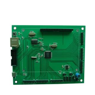
In the manufacturing and assembly of printed circuit boards (PCBs), mark points (also known as fiducial marks) play a critical role in ensuring precise component placement. These reference points enable automated assembly equipment, such as pick-and-place machines and optical inspection systems, to accurately align PCBs during production. Improperly designed or placed mark points can lead to misalignment, defective soldering, and reduced manufacturing yield.
This article provides comprehensive guidelines for the standardized design and placement of PCB mark points, covering their types, dimensions, positioning, and material considerations to optimize assembly accuracy and efficiency.
2. Types of PCB Mark Points
There are two primary types of mark points used in PCB assembly:
2.1 Global Fiducial Marks
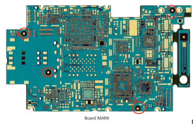
Global fiducial marks serve as reference points for the entire PCB. They are typically placed near the board corners and are used by assembly machines to determine the PCB’s position and orientation.
Key Characteristics:
- Minimum of two marks (preferably three for redundancy).
- Symmetrically placed to avoid rotational errors.
- Used in both surface-mount technology (SMT) and through-hole assembly.
2.2 Local Fiducial Marks
Local fiducial marks are specific to individual components, particularly fine-pitch devices such as Ball Grid Arrays (BGAs), Quad Flat Packages (QFPs), and other high-density components. They help machines precisely align these components during placement.
Key Characteristics:
- Placed near the component (usually diagonal to it).
- Required for components with a pitch ≤ 0.5mm.
- Used to compensate for PCB warping or slight misalignment.

3. Design Specifications for Mark Points
3.1 Shape and Size
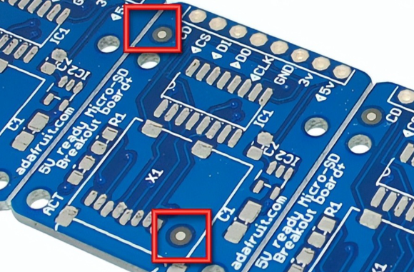
Mark points are typically circular, as this shape provides the best contrast and detection reliability for vision systems.
Recommended Dimensions:
- Diameter: 1.0mm to 3.0mm (optimal: 1.5mm).
- Minimum Clearance: A clear area (no copper or solder mask) should surround the mark point, with a diameter at least twice the mark’s size (e.g., 3.0mm clearance for a 1.5mm mark).
3.2 Material and Contrast
For optimal machine recognition, mark points must provide high contrast against the PCB background.
Best Practices:
- Copper-Based Marks: Exposed copper (with anti-oxidation coating) on a non-contrasting background.
- Solder Mask-Defined Marks: Bare copper surrounded by solder mask (most common).
- Avoid: Silk-screen printing over mark points, as it reduces contrast.
3.3 Layer Placement
Mark points should be placed on both the top and bottom layers if double-sided assembly is required.
Guidelines:
- For single-sided assembly, only top-layer marks are needed.
- For double-sided assembly, ensure mark points on both layers are aligned to prevent misregistration.
4. Placement Guidelines
4.1 Global Fiducial Mark Placement
- Number of Marks: At least two, preferably three (to detect rotation errors).
- Positioning: Near opposite corners (e.g., top-left and bottom-right).
- Distance from Board Edge: ≥ 5mm to avoid interference with panel rails or clamping mechanisms.
4.2 Local Fiducial Mark Placement
- For BGAs/QFPs: Two diagonal marks near the component (within 10mm).
- Avoid Obstructions: Ensure no traces, vias, or components obstruct the camera’s view.
4.3 Panelized PCB Considerations
In panelized PCBs (multi-board arrays), fiducial marks should be placed:
- On each individual PCB (for depaneling accuracy).
- On the panel rails (for overall alignment).
5. Inspection and Verification
5.1 Automated Optical Inspection (AOI) Compatibility
- Ensure mark points are detectable by AOI systems (proper contrast, no blurring).
- Avoid reflective finishes that may cause glare.
5.2 Tolerance and Accuracy
- Placement Tolerance: ±0.05mm for high-precision assemblies.
- Size Consistency: All marks on a PCB should have identical dimensions.
6. Common Mistakes and How to Avoid Them
6.1 Insufficient Clearance
- Issue: Traces or solder mask too close to the mark point.
- Solution: Maintain a clear annular ring around the mark.
6.2 Poor Contrast
- Issue: Low contrast due to incorrect surface finish.
- Solution: Use bare copper with a solder mask or ENIG finish.
6.3 Incorrect Quantity or Placement
- Issue: Only one global fiducial (leading to rotational errors).
- Solution: Always use at least two (preferably three) marks.
7. Conclusion
Properly designed and placed mark points are essential for high-yield PCB assembly. By adhering to standardized dimensions, contrast requirements, and positioning guidelines, manufacturers can ensure reliable automated assembly and inspection. Implementing these best practices minimizes placement errors, reduces rework, and improves overall production efficiency.
Following IPC-7351 and other industry standards ensures compatibility with modern assembly equipment, making mark point optimization a critical step in PCB design for manufacturability (DFM).