Talk about the reliability principles of circuit design and PCB wiring that you don’t know
Talk about the reliability principles of circuit design and PCB wiring that you don’t know
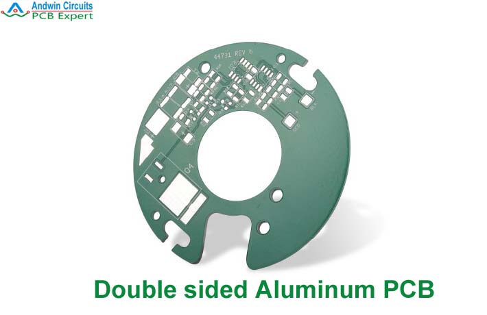
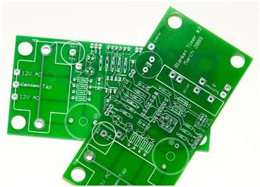
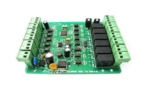
At present, electronic equipment used in various electronic equipment and systems still uses printed circuit boards as the main assembly method. Practice has proved that even if the circuit schematic is designed correctly, improper printed circuit board design will have an adverse effect on the reliability of electronic equipment.
Therefore, when designing printed circuit boards, you should pay attention to using the correct method.
1.Grounding
Ground wire design In electronic equipment, grounding is an important method to control interference. If grounding and shielding can be used correctly, most interference problems can be solved. The ground wire structure in electronic equipment generally includes system ground, chassis ground (shielded ground), digital ground (logic ground) and analog ground.
The following points should be noted in ground wire design
Correctly choose single-point grounding and multi-point grounding In low-frequency circuits, the operating frequency of the signal is less than 1MHz, and its wiring and the inductance between devices have little effect, while the loop formed by the grounding circuit has a greater impact on interference, so one-point grounding should be used. When the signal operating frequency is greater than 10MHz, the ground wire impedance becomes very large.
At this time, the ground wire impedance should be reduced as much as possible, and multi-point grounding should be used nearby. When the operating frequency is between 1 and 10 MHz, if one-point grounding is used, the length of the ground wire should not exceed 1/20 of the wavelength, otherwise a multi-point grounding method should be used.
Separate digital circuits from analog circuits.
There are both high-speed logic circuits and linear circuits on the circuit board. They should be separated as much as possible, and the ground wires of the two should not be mixed. They should be connected to the ground wires of the power supply end respectively. The grounding area of the linear circuit should be increased as much as possible.
Thicken the ground wire as much as possible.
If the ground wire is very thin, the ground potential will change with the change of current, causing the timing signal level of the electronic equipment to be unstable and the anti-noise performance to deteriorate. Therefore, the ground wire should be as thick as possible so that it can pass the allowable current of the three-point printed circuit board. If possible, the width of the ground wire should be greater than 3mm.
Constitute the ground wire into a closed loop.
When designing the ground wire system of a printed circuit board composed only of digital circuits, making the ground wire into a closed loop can significantly improve the anti-noise ability. The reason is that there are many integrated circuit components on the printed circuit board, especially when there are components that consume a lot of power. Due to the limitation of the thickness of the grounding wire, a large potential difference will be generated on the ground junction, causing the anti-noise ability to decrease. If the grounding structure is formed into a loop, the potential difference will be reduced, and the anti-noise ability of the electronic equipment will be improved.
2.Electromagnetic compatibility design
Electromagnetic compatibility refers to the ability of electronic equipment to work in a coordinated and effective manner in various electromagnetic environments. The purpose of electromagnetic compatibility design is to enable electronic equipment to suppress various external interferences, so that electronic equipment can work normally in a specific electromagnetic environment, and at the same time reduce the electromagnetic interference of electronic equipment itself to other electronic equipment.
Choose a reasonable wire width.
Since the impact interference generated by transient current on the printed line is mainly caused by the inductance component of the printed wire, the inductance of the printed wire should be minimized. The inductance of the printed wire is proportional to its length and inversely proportional to its width. Therefore, short and fine wires are beneficial to suppress interference. The signal lines of clock leads, row drivers or bus drivers often carry large transient currents, and the printed wires should be as short as possible. For discrete component circuits, the requirements can be fully met when the printed conductor width is about 1.5mm; for integrated circuits, the printed conductor width can be selected between 0.2 and 1.0mm.
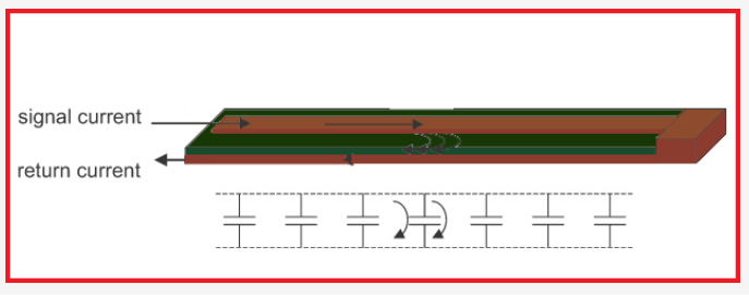
Using the correct wiring strategy, equal routing can reduce the conductor inductance, but the mutual inductance and distributed capacitance between the conductors increase. If the layout allows, it is best to use a tic-tac-toe mesh wiring structure. The specific method is to wire horizontally on one side of the printed board and vertically on the other side, and then connect them with metallized holes at the cross holes.
In order to suppress crosstalk between the conductors of the printed board, long-distance equal routing should be avoided as much as possible when designing the wiring, and the distance between the lines should be kept as far as possible. The signal line should not cross the ground line and the power line as much as possible. Setting a grounded printed line between some signal lines that are very sensitive to interference can effectively suppress crosstalk. To avoid electromagnetic radiation when high-frequency signals pass through printed conductors, please note:
Try to minimize the discontinuity of printed conductors, such as the conductor width should not change suddenly, the corner of the conductor should be greater than 90 degrees, and loop routing is prohibited.
Clock signal leads are most likely to generate electromagnetic radiation interference. When routing, they should be close to the ground loop, and the driver should be close to the connector.
The bus driver should be close to the bus it wants to drive. For those leads that leave the printed circuit board, the driver should be close to the connector.
The data bus wiring should sandwich a signal ground wire between every two signal lines.
It is best to place the ground loop close to the least important address lead, because the latter often carries high-frequency current.
When arranging high-speed, medium-speed and low-speed logic circuits on the printed board, arrange the devices 3. Suppress reflection interference In order to suppress the reflection interference that appears at the terminal of the printed line, except for special needs, the length of the printed line should be shortened as much as possible and a slow circuit should be used. If necessary, terminal matching can be added, that is, a matching resistor of the same resistance value is added to the ground and power supply ends at the end of the transmission line. According to experience, for TTL circuits with generally faster speeds, terminal matching measures should be adopted when the printed lines are longer than 10cm. The resistance value of the matching resistor should be determined according to the maximum value of the output drive current and absorption current of the integrated circuit.

3.Decoupling capacitor configuration
In the DC power supply circuit, changes in load will cause power supply noise. For example, in a digital circuit, when the circuit switches from one state to another, a large peak current will be generated on the power line, forming a transient noise voltage. Configuring decoupling capacitors can suppress the noise caused by load changes, which is a common practice for the reliability design of printed circuit boards.
The configuration principles are as follows:
A 10~100uF electrolytic capacitor is connected across the power input end. If the position of the printed circuit board allows, the anti-interference effect of using an electrolytic capacitor of more than 100uF will be better.
Configure a 0.01uF ceramic capacitor for each integrated circuit chip.
If the printed circuit board space is small and cannot be installed, a 1~10uF tantalum electrolytic capacitor can be configured for every 4~10 chips. The high-frequency impedance of this device is particularly small, and the impedance is less than 1Ω in the range of 500kHz~20MHz, and the leakage current is very small (below 0.5uA).
For devices with weak noise resistance, large current changes when turned off, and storage devices such as ROM and RAM, decoupling capacitors should be directly connected between the power line (Vcc) and the ground line (GND) of the chip.
The lead of the decoupling capacitor should not be too long, especially the high-frequency bypass capacitor should not have a lead
4. the size of the printed circuit board and the layout of the device
The size of the printed circuit board should be moderate. If it is too large, the printed lines are long and the impedance increases, which not only reduces the anti-noise ability but also increases the cost; if it is too small, the heat dissipation is not good and it is easily interfered by the adjacent lines.
In terms of device layout, like other logic circuits, related devices should be placed as close as possible to obtain better anti-noise effect. The clock generator, crystal oscillator and the clock input of the CPU are all prone to noise, so they should be closer to each other. Devices that are prone to noise, small current circuits, large current circuits, etc. should be kept as far away from the logic circuit as possible. If possible, a separate circuit board should be made. This is very important.
5.Thermal design starts from the perspective of heat dissipation
It is best to install the printed board vertically. The distance between the boards should generally not be less than 2cm, and the arrangement of the devices on the printed board should follow certain rules:
For equipment using free convection air cooling, it is best to arrange the integrated circuits (or other devices) in a longitudinal manner;
For equipment using forced air cooling, it is best to arrange the integrated circuits (or other devices) in a horizontal manner;
The devices on the same printed board should be arranged according to their heat generation and heat dissipation as much as possible.
Devices with low heat generation or poor heat resistance (such as small signal transistors, small-scale integrated circuits) should be arranged horizontally. Circuits, electrolytic capacitors, etc.) are placed at the uppermost stream (entrance) of the cooling airflow, and devices with high heat generation or good heat resistance (such as power transistors, large-scale integrated circuits, etc.) are placed at the lowest downstream of the cooling airflow;
In the horizontal direction, high-power devices are arranged as close to the edge of the printed circuit board as possible to shorten the heat transfer path;
In the vertical direction, high-power devices are arranged as close to the top of the printed circuit board as possible to reduce the impact of these devices on the temperature of other devices when they are working;
Device that is sensitive to temperature is best placed in the lowest temperature area (such as the bottom of the equipment), and it must not be placed directly above the heating device. Multiple devices are best arranged in a staggered manner on the horizontal plane;