The Advantages and Disadvantages of Copper-Poured PCB Design
Introduction
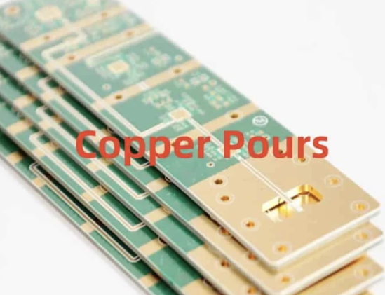
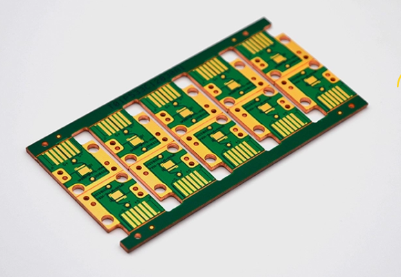
Printed Circuit Board (PCB) design is a critical aspect of electronic engineering, influencing the performance, reliability, and manufacturability of electronic devices. One common technique used in PCB design is copper pouring (also known as copper fill or copper flooding), where large areas of the PCB are covered with copper connected to a ground or power net. This method has both benefits and drawbacks, affecting signal integrity, thermal management, and electromagnetic compatibility (EMC).
This article explores the advantages and disadvantages of copper-poured PCB design, providing insights into when and how to use this technique effectively.
Advantages of Copper-Poured PCB Design
1. Improved Thermal Management
Copper is an excellent conductor of heat, and copper pours help dissipate heat generated by high-power components such as voltage regulators, processors, and power amplifiers. By connecting copper pours to ground or power planes, designers can enhance heat distribution, reducing the risk of overheating and improving the PCB’s thermal performance.
- Heat Spreading: Large copper areas act as heat sinks, spreading thermal energy across the board.
- Reduced Hotspots: Prevents localized overheating, increasing component lifespan.
2. Enhanced Signal Integrity and Reduced Noise
Copper pours help in maintaining signal integrity by:
- Reducing Ground Loops: A solid ground plane minimizes return path discontinuities, lowering electromagnetic interference (EMI).
- Shielding Sensitive Traces: Copper acts as a shield against crosstalk and external noise, especially in high-frequency designs.
- Lowering Impedance: Provides a low-impedance return path for high-speed signals, reducing signal distortion.
3. Better Electromagnetic Compatibility (EMC)
Copper pours contribute to EMC by:
- Reducing Radiated Emissions: Large copper areas minimize loop antennas that can emit electromagnetic radiation.
- Improving Immunity: Shielding sensitive circuits from external RF interference.
4. Improved Manufacturing Yield and Reliability
- Even Copper Distribution: Helps prevent uneven etching and warping during PCB fabrication.
- Reduced Risk of Delamination: Uniform copper distribution enhances structural integrity.
5. Lower Impedance Power Distribution
- Copper pours connected to power nets reduce voltage drops and improve power delivery efficiency.
Disadvantages of Copper-Poured PCB Design
Despite its benefits, copper pouring can introduce several challenges if not implemented carefully.
1. Increased Parasitic Capacitance
- Copper pours near high-speed signal traces can introduce parasitic capacitance, leading to signal degradation, especially in high-frequency circuits (>100 MHz).
- Solution: Use spaced copper fills or avoid pouring copper under critical signal paths.
2. Potential for Ground Loops (If Poorly Designed)
- If multiple ground connections create unintended loops, they can act as antennas, increasing EMI.
- Solution: Ensure a well-designed ground plane with proper stitching vias.
3. Difficulty in Rework and Debugging
- Large copper areas make it harder to cut traces or isolate components during debugging.
- Solution: Leave small gaps or use thermal relief connections for through-hole components.
4. Increased Complexity in High-Density Designs
- Copper pours can complicate routing in tightly packed PCBs, leading to unintended short circuits.
- Solution: Use design rules (DRC) to enforce proper clearances.
5. Potential for Acid Traps in Manufacturing
- Small isolated copper islands can trap etching chemicals, leading to manufacturing defects.
- Solution: Use “teardrops” or remove orphaned copper sections.

Best Practices for Copper-Poured PCB Design
To maximize benefits while minimizing drawbacks, follow these guidelines:
- Use a Structured Ground Plane
- Ensure a continuous ground plane beneath high-speed signals.
- Avoid splitting ground planes unnecessarily.
- Control Copper Pour Clearance
- Maintain sufficient spacing between copper pours and signal traces (e.g., 0.2mm–0.5mm).
- Implement Thermal Relief Pads
- Prevents poor soldering due to excessive heat dissipation.
- Avoid Floating Copper Islands
- Remove or connect all copper sections to a net to prevent EMI issues.
- Optimize for High-Frequency Signals
- Use hatched copper pours to reduce parasitic capacitance in RF designs.
Conclusion
Copper pouring is a powerful technique in PCB design, offering significant advantages in thermal management, signal integrity, and EMC performance. However, it also introduces challenges such as parasitic capacitance, manufacturing complexities, and potential ground loops.
By following best practices—such as maintaining proper clearances, using thermal reliefs, and ensuring a solid ground plane—designers can leverage copper pours effectively while mitigating their drawbacks.
Ultimately, the decision to use copper pouring should be based on the specific requirements of the PCB, balancing performance, manufacturability, and cost considerations.