The Composition Elements of PCB Packaging: A Comprehensive Guide
Introduction to PCB Packaging
Printed Circuit Board (PCB) packaging serves as the critical interface between electronic components and the circuit board itself. It provides the mechanical structure for mounting components while establishing electrical connections through conductive pathways. PCB packaging has evolved significantly alongside electronic miniaturization and increasing complexity, with modern packages accommodating everything from simple resistors to advanced microprocessors.
Understanding the composition elements of PCB packaging is essential for electronics designers, PCB layout engineers, and manufacturing professionals. These elements determine not only how components connect to the board but also influence electrical performance, thermal management, manufacturing yield, and product reliability. This article provides a detailed examination of the fundamental elements that constitute PCB packaging.
1. Physical Structure Elements
1.1 Lead Frames
Lead frames form the foundational structure of many PCB packages, particularly for integrated circuits (ICs). These thin metal structures, typically made from copper alloys or Alloy 42 (an iron-nickel alloy), serve multiple purposes:
- Mechanical Support: Provides structural integrity for the semiconductor die
- Electrical Pathways: Creates conductive paths between the die and external connections
- Heat Dissipation: Acts as a thermal conduit for heat generated by the component
Lead frames can be categorized into:
- Single-row frames (used in SIP, DIP packages)
- Dual-row frames (common in QFP packages)
- Array-type frames (for BGA and LGA packages)
Modern lead frames often feature sophisticated designs with downset paddles for die attachment and precisely formed leads for optimal soldering.
1.2 Substrates
For advanced packaging, especially in ball grid array (BGA) and chip-scale packages (CSP), substrates replace traditional lead frames. These substrates are typically composed of:
- Organic substrates: Laminate materials like bismaleimide-triazine (BT) resin or epoxy-based materials with copper traces
- Ceramic substrates: Used in high-reliability applications for their excellent thermal and mechanical properties
- Silicon interposers: Employed in 2.5D and 3D packaging for fine-pitch interconnections
Substrates incorporate multiple layers of conductive traces and vias to route signals from the component to the PCB while providing mechanical support.
1.3 Encapsulation Materials
Encapsulation serves to protect the delicate semiconductor die and internal connections from environmental factors. Common encapsulation materials include:
- Epoxy molding compounds (EMC): Thermoset polymers filled with silica for enhanced properties
- Liquid encapsulants: Used in glob-top and underfill applications
- Hermetic ceramic/metal packages: For high-reliability military and aerospace applications
Encapsulation materials must balance multiple properties including thermal conductivity, coefficient of thermal expansion (CTE) matching, moisture resistance, and electrical insulation.
2. Electrical Connection Elements
2.1 Bonding Wires
Wire bonding remains the most common method for connecting semiconductor dies to packages. The three primary wire bonding technologies are:
- Gold wire bonding: Uses thermosonic bonding with gold wires (typically 0.7-2 mil diameter)
- Copper wire bonding: Lower cost alternative to gold with better electrical conductivity
- Aluminum wedge bonding: Used for power devices and high-current applications
Wire bonds create electrical connections between bond pads on the die and the lead frame or substrate.
2.2 Solder Balls and Bumps
For flip-chip and area array packages, solder interconnects replace wire bonds:
- C4 (Controlled Collapse Chip Connection): High-lead solder bumps for flip-chip attachment
- Lead-free solder balls: Typically SAC alloys (Sn-Ag-Cu) for BGA packages
- Microbumps: Extremely small solder connections (25-50μm) for 3D IC stacking
These connections provide both electrical pathways and mechanical attachment while allowing for thermal expansion differences between components.
2.3 Lead Configurations
The external connection methods vary significantly by package type:
- Through-hole leads: Axial and radial leads for insertion mounting
- Gull-wing leads: Used in surface-mount packages like SOIC and QFP
- J-leads: For PLCC and other surface-mount packages
- No-lead configurations: Such as QFN (Quad Flat No-lead) packages with perimeter pads
- Area array contacts: Solder balls in BGA and LGA packages
Each lead type presents different considerations for PCB layout, soldering processes, and mechanical reliability.
3. Thermal Management Elements
3.1 Thermal Pads and Slugs
Many power packages incorporate dedicated thermal conduction paths:
- Exposed pads: Copper surfaces on the package bottom for direct heat sinking
- Integrated heat spreaders: Metal lids that conduct heat away from the die
- Thermal vias: Arrays of conductive vias under packages to transfer heat to PCB layers
3.2 Heat Spreader Materials
Advanced packages often include:
- Copper heat spreaders: For high thermal conductivity
- Graphite-based materials: For anisotropic thermal management
- Vapor chambers: In some high-power modules
4. Mechanical and Structural Elements
4.1 Package Body
The main structural component that houses all other elements:
- Plastic molded bodies: Most common for commercial components
- Ceramic packages: For high-frequency or high-reliability applications
- Metal cans: Historically used for discrete transistors and some RF devices
4.2 Lid and Shield
Some packages feature:
- Metal lids: For electromagnetic shielding or hermetic sealing
- Shielding cans: Soldered to PCB to create shielded compartments
5. Marking and Identification Elements
5.1 Component Markings
Essential for identification and traceability:
- Laser marking: For permanent component identification
- Ink marking: Less expensive but less durable
- Embossing: Used on some molded packages
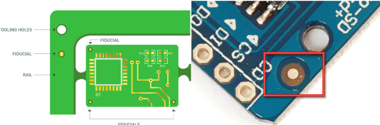
5.2 Polarity Indicators
Critical for proper orientation:
- Dots, notches, and bevelled edges: For IC orientation
- Band markings: On diodes and polarized capacitors
- Pin 1 indicators: Various forms for different package types
6. Special Features in Advanced Packaging
Modern packaging technologies incorporate additional elements:
6.1 Interposers
Used in 2.5D packaging to facilitate high-density interconnects:
- Silicon interposers: With through-silicon vias (TSVs)
- Organic interposers: Lower cost alternatives
6.2 Embedded Components
Some advanced packages incorporate:
- Passive components: Resistors, capacitors within the package
- Multiple dies: System-in-Package (SiP) configurations
6.3 Optical Interfaces
For optoelectronic packages:
- Lens elements: For LED and photodiode packages
- Fiber alignment features: In optical communication components
Conclusion
PCB packaging comprises a complex interplay of structural, electrical, thermal, and mechanical elements that collectively determine component performance and reliability. From traditional leaded packages to advanced system-in-package solutions, each packaging approach combines these fundamental elements in different configurations to meet specific application requirements.
As electronics continue advancing toward higher frequencies, greater miniaturization, and increased functionality, PCB packaging will continue evolving. Emerging technologies like fan-out wafer-level packaging (FOWLP), 3D IC stacking, and heterogeneous integration are pushing the boundaries of traditional packaging concepts. However, these innovations still build upon the fundamental elements discussed in this article—properly understanding these building blocks remains essential for effective electronic design and manufacturing.
For engineers and designers, mastering PCB packaging elements enables better component selection, optimized board layout, and improved manufacturing outcomes. As the bridge between silicon and system, packaging will remain a critical focus area in electronics development for the foreseeable future.