The Comprehensive Guide to PCB Stencils: Design, Types, and Best Practices
Introduction to PCB Stencils
Printed Circuit Board (PCB) stencils, also known as solder paste stencils, are fundamental tools in modern electronics manufacturing. These precision tools serve as the bridge between PCB design and physical assembly, enabling the accurate deposition of solder paste onto circuit boards prior to component placement.
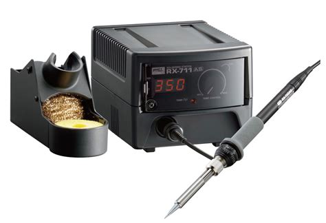
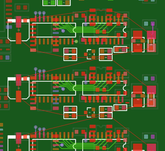
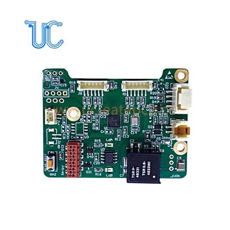
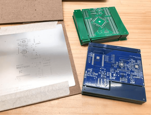
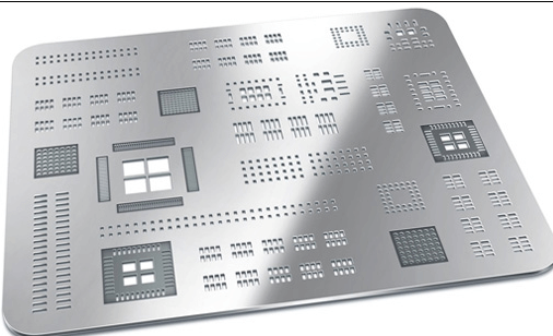
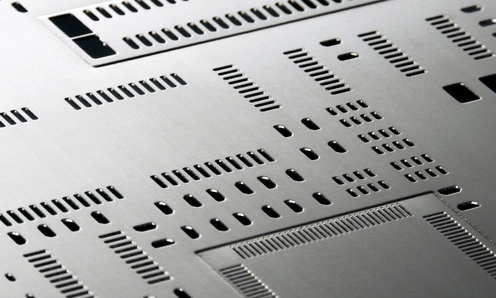
A PCB stencil is essentially a thin sheet of material (typically stainless steel) with laser-cut openings that correspond to the solder pads on a PCB. When aligned properly over the board, solder paste is applied across the stencil surface, filling these openings and transferring precise amounts of paste onto each pad. This process is critical for Surface Mount Technology (SMT) assembly, where components are placed directly onto these solder paste deposits before the entire assembly goes through a reflow oven to create permanent solder joints.
The importance of PCB stencils in electronics manufacturing cannot be overstated. They directly impact:
- Assembly quality and reliability
- Production efficiency
- Yield rates
- Miniaturization capabilities
- Process consistency
As electronic devices continue to shrink in size while growing in complexity, the role of PCB stencils becomes even more crucial. Modern designs with fine-pitch components (some with pitches below 0.4mm) and high-density interconnects demand exceptional precision in solder paste application—a requirement that only well-designed and properly manufactured stencils can meet.
Types of PCB Stencils
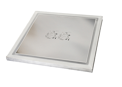
Framed Stencils
Framed stencils are the most common type used in medium to high-volume production environments. These stencils consist of a metal foil (typically stainless steel) tensioned and bonded to a rigid frame, usually made of aluminum. The frame provides stability and ensures the stencil remains flat during the printing process.
Advantages:
- Excellent stability and tension maintenance
- Compatible with automatic stencil printers
- Long lifespan with proper care
- Consistent performance over many print cycles
Disadvantages:
- Higher initial cost
- Bulkier storage requirements
- Less practical for prototype or low-volume work
Framed stencils are ideal for production runs where the same PCB design will be assembled repeatedly. They typically offer the highest print quality and consistency for volume manufacturing.
Frameless Stencils
Frameless stencils, as the name suggests, lack the permanent frame of their counterparts. Instead, they consist of just the metal foil, which is temporarily clamped into a reusable frame during the printing process.
Advantages:
- Lower cost (especially for prototypes)
- Compact storage
- Easy to modify or adapt
- Quick turnaround times
Disadvantages:
- Requires compatible stencil printer
- May lack tension consistency of framed stencils
- Generally shorter lifespan
Frameless stencils are particularly useful for:
- Prototype development
- Low-volume production
- Research and development environments
- Educational purposes
Laser-Cut Stencils
Laser-cut stencils represent the gold standard in PCB stencil manufacturing. Created using high-precision laser systems, these stencils offer exceptional accuracy and edge quality.
Key Features:
- Typical accuracy: ±0.01mm or better
- Smooth aperture walls reduce paste sticking
- Capable of handling fine-pitch components (down to 0.3mm pitch)
- Suitable for both leaded and lead-free solder pastes
Laser cutting allows for precise control over aperture geometry, enabling designers to create optimized shapes for different component types. The process is computer-controlled, ensuring perfect alignment with the PCB design files.
Chemical-Etched Stencils
Chemical etching is an older stencil manufacturing technique that uses chemical baths to remove material and create apertures.
Characteristics:
- Lower cost compared to laser cutting
- Faster production for simple designs
- Hourglass-shaped aperture profile (wider in middle than at top/bottom)
- Limited to simpler designs with larger features
While chemical etching can be adequate for some through-hole applications or larger SMT components, it generally cannot achieve the precision needed for modern high-density designs. The process also tends to create rougher aperture walls that can impede solder paste release.
Electroformed Stencils
Electroformed stencils are created through a nickel plating process that builds up the stencil material around a patterned mandrel.
Unique Attributes:
- Extremely smooth aperture walls
- Consistent thickness throughout
- Ability to create stepped stencils (varying thickness)
- Excellent for ultra-fine pitch applications
The electroforming process allows for particularly good solder paste release characteristics, making these stencils valuable for challenging applications. However, they are typically the most expensive option and have longer lead times.
PCB Stencil Design Considerations
Aperture Design
Aperture design is perhaps the most critical aspect of PCB stencil engineering. The size, shape, and wall profile of each opening directly affects how solder paste transfers to the PCB.
Key Parameters:
- Aperture Size: Generally 1:1 with pad size for most components
- Aspect Ratio: Opening width vs. stencil thickness (should be >1.5 for good release)
- Area Ratio: Opening area vs. wall area (should be >0.66 for good release)
- Shape: Typically matches pad shape, but can be modified for special needs
For fine-pitch components (below 0.5mm pitch), designers often use slightly reduced apertures (90-95% of pad size) to prevent bridging. Conversely, for large components like QFPs or BGAs, apertures might be modified with special shapes (home plate, bowtie) to ensure proper solder volume distribution.
Stencil Thickness
Stencil thickness is a primary determinant of how much solder paste gets deposited. Common thicknesses include:
- 0.1mm (4mil): For ultra-fine pitch components
- 0.12mm (5mil): General purpose for modern SMT
- 0.15mm (6mil): For larger components or mixed technology boards
- 0.2mm (8mil): Primarily for through-hole components with paste-in-hole process
Selecting the proper thickness involves balancing:
- Solder volume requirements for different components
- The finest pitch on the board
- PCB surface planarity
- Solder paste characteristics
In some cases, stepped stencils (with areas of different thickness) are used to accommodate varying requirements across a single PCB.
Fiducial Marks and Alignment
Fiducial marks are crucial reference points that ensure proper alignment between the stencil and PCB. These typically consist of:
- Global Fiducials: Usually 2-3 marks for overall board alignment
- Local Fiducials: For critical components or high-density areas
Design guidelines for fiducials:
- Minimum diameter of 1mm
- Clear keep-out area around each fiducial
- Symmetrical placement when possible
- Copper-defined rather than solder mask-defined
Proper fiducial design becomes increasingly important as component sizes shrink and placement tolerances tighten.
Stencil Material Selection
While stainless steel dominates the PCB stencil market, material choice affects performance:
Stainless Steel (Most Common):
- 300-series (304, 316) most popular
- Excellent durability
- Good release characteristics with proper coating
- Typical thickness range: 0.05mm to 0.2mm
Nickel (for Electroformed Stencils):
- Superior smoothness
- Natural release properties
- More expensive
- Less durable than steel
Polyimide (for Temporary/Prototype Use):
- Low cost
- Fast turnaround
- Very limited lifespan
- Poor performance with fine features
Material selection should consider:
- Expected production volume
- Smallest feature size
- Solder paste type
- Cleaning requirements
PCB Stencil Manufacturing Process
Laser Cutting Technology
Modern laser cutting systems offer exceptional precision for PCB stencil manufacturing. The process typically involves:
- File Preparation: Converting Gerber or CAD data to cutting paths
- Material Loading: Mounting the stainless steel sheet
- Laser Cutting: Using high-power lasers (usually fiber) to vaporize material
- Cleaning: Removing debris and slag
- Inspection: Verifying dimensions and quality
Advanced systems feature:
- Real-time power adjustment for consistent cuts
- Automatic focus control
- Vision systems for alignment verification
- Cutting speeds up to 500mm/sec
Laser cutting can achieve:
- Positional accuracy: ±10μm
- Aperture size accuracy: ±5μm
- Minimum feature size: 50μm
- Edge roughness: <5μm Ra
Electroforming Process
Electroformed stencils undergo a completely different manufacturing approach:
- Mandrel Preparation: Creating a patterned master
- Nickel Deposition: Building up nickel layer by layer
- Release: Separating the formed stencil from the mandrel
- Trimming and Framing: Final sizing and mounting
This additive process allows for unique features like:
- Perfectly smooth aperture walls
- Precise thickness control (±2μm)
- Tapered or stepped profiles
- Integrated nano-coatings
Quality Control Measures
Regardless of manufacturing method, rigorous quality control is essential:
Dimensional Verification:
- Optical measurement systems
- Automated inspection against design files
- Cross-section analysis for critical apertures
Surface Quality Checks:
- Roughness measurements
- Defect detection (burrs, slag)
- Coating uniformity (if applied)
Functional Testing:
- Solder paste transfer efficiency tests
- Release performance evaluation
- Print trials on actual PCBs
Industry standards like IPC-7525 provide guidelines for stencil design and quality requirements, helping ensure consistent performance across manufacturers.
PCB Stencil Applications
SMT Assembly
The primary application of PCB stencils is in SMT assembly lines, where they enable:
High-Speed Printing:
- Modern stencil printers can achieve >20,000 prints per day
- Cycle times under 10 seconds per board
- Consistent deposition across the production run
Fine-Pitch Capability:
- 01005 chip components (0.4×0.2mm)
- 0.3mm pitch QFNs and BGAs
- MicroBGAs and CSPs
Mixed Technology:
- Combining various component sizes on one board
- Accommodating different solder volume needs
- Supporting leaded and lead-free pastes simultaneously
Prototype Development
PCB stencils play a vital role in prototype development by:
Enabling Rapid Iteration:
- Quick-turn stencil availability (often 24 hours)
- Low-cost frameless options for testing
- Easy modification between design versions
Supporting Design Validation:
- Verifying component footprints
- Testing solder joint reliability
- Evaluating thermal performance
Facilitating Small-Batch Production:
- Bridge tooling before volume production
- Pilot runs for process development
- Custom or niche product manufacturing
Rework and Repair
Specialized stencils assist in rework scenarios:
Localized Stencils:
- For individual component replacement
- Mini stencils for BGA reballing
- Targeted solder paste application
Step Stencils:
- Adding solder to existing joints
- Correcting insufficient solder volume
- Repairing lifted pads or traces
These application-specific stencils help maintain quality standards while minimizing material waste during rework operations.
Best Practices for PCB Stencil Usage
Proper Handling and Storage
To maximize stencil lifespan and performance:
Handling Guidelines:
- Always wear gloves to prevent contamination
- Support the stencil evenly when moving
- Avoid flexing or bending the foil
- Use proper lifting techniques for framed stencils
Storage Recommendations:
- Vertical storage in climate-controlled environments
- Protective covers or sleeves when not in use
- Designated racks to prevent stacking damage
- Clean before storage to prevent paste hardening
Cleaning Procedures
Regular cleaning is essential for consistent print quality:
Daily Cleaning:
- Wipe both sides with lint-free wipes
- Use approved stencil cleaners
- Visual inspection under magnification
Deep Cleaning:
- Ultrasonic cleaning for stubborn deposits
- Specialized cleaning solutions
- Complete drying before reuse
Frequency Guidelines:
- Every 10-15 prints for lead-free pastes
- Every 20-30 prints for leaded pastes
- Immediately after any print quality issues
Process Optimization
Achieving optimal print results requires attention to:
Squeegee Parameters:
- Pressure (typically 0.5-1.5kg/cm)
- Angle (usually 45-60°)
- Speed (10-50mm/sec depending on paste)
- Material (metal or polyurethane)
Print Gap Settings:
- Zero gap for most applications
- Small gap for warped boards
- Consistent across entire print area
Environmental Controls:
- Temperature (20-25°C ideal)
- Humidity (40-60% RH)
- Minimized air flow to prevent paste drying
Regular process verification using print quality metrics helps maintain consistent results throughout production runs.
Advanced PCB Stencil Technologies
Nano-Coated Stencils
Nano-coatings enhance stencil performance through:
Improved Release Characteristics:
- Reduced adhesion to solder paste
- Smoother paste flow through apertures
- Less frequent cleaning required
Durability Enhancements:
- Increased resistance to wear
- Better chemical resistance
- Longer coating lifespan
Common coating materials include:
- PTFE-based formulations
- Silicon nitride
- Diamond-like carbon (DLC)
3D/Step Stencils
3D stencils feature varying thickness to address:
Mixed Component Requirements:
- Thicker areas for large components
- Standard thickness for most SMT
- Thin sections for fine-pitch devices
Special Applications:
- Edge connectors
- Press-fit components
- Shielding cans
Creation methods include:
- Laser cutting with depth control
- Selective electroforming
- Precision etching techniques
Smart Stencils
Emerging technologies are bringing intelligence to stencils:
Embedded Sensors:
- Tension monitoring
- Temperature sensing
- Wear detection
Adaptive Features:
- Self-cleaning surfaces
- Dynamic aperture adjustment
- Real-time print quality feedback
While most of these are still in development, they represent the future of stencil technology as Industry 4.0 transforms electronics manufacturing.
Troubleshooting Common PCB Stencil Issues
Solder Paste Release Problems
Poor paste release manifests as:
Symptoms:
- Incomplete paste deposits
- Ragged or peaked paste mounds
- Variable paste volumes
Solutions:
- Verify aspect and area ratios meet guidelines
- Consider nano-coated stencils
- Optimize squeegee parameters
- Evaluate paste rheology
Stencil Clogging
Clogged apertures cause:
Indicators:
- Missing or incomplete deposits
- Visible paste buildup in apertures
- Increasing defects over consecutive prints
Remedies:
- Implement more frequent cleaning
- Use appropriate cleaning methods
- Consider smaller aperture sizes
- Evaluate paste metal content
Misalignment Issues
Alignment problems result in:
Effects:
- Off-center paste deposits
- Bridging between pads
- Poor component placement
Corrective Actions:
- Verify fiducial quality and quantity
- Check stencil tension (for framed stencils)
- Inspect printer vision system
- Confirm PCB fabrication accuracy
Future Trends in PCB Stencil Technology
Miniaturization Demands
As components continue shrinking, stencil technology must adapt:
Challenges:
- 008004 components (0.25×0.125mm) becoming common
- Sub-0.3mm pitch devices
- Increased density with heterogeneous integration
Innovations:
- Improved laser systems with smaller spot sizes
- Advanced coatings for micron-scale features
- Novel materials with higher strength-to-thickness ratios
Sustainable Manufacturing
Environmental considerations are driving changes:
Eco-Friendly Materials:
- Recyclable stencil substrates
- Bio-based coatings
- Reduced chemical usage in manufacturing
Process Optimizations:
- Longer-lasting stencils to reduce waste
- Energy-efficient production methods
- Closed-loop cleaning systems
Digital Integration
The smart factory revolution impacts stencils through:
Industry 4.0 Connectivity:
- Stencils with embedded RFID for tracking
- Cloud-based stencil management systems
- Predictive maintenance based on usage data
Advanced Process Control:
- Real-time print monitoring
- Automated adjustment based on feedback
- Machine learning for defect prevention
Conclusion
PCB stencils remain indispensable tools in electronics manufacturing, bridging the gap between design and physical reality. As the industry evolves toward smaller, more complex, and more reliable electronic assemblies, stencil technology continues to advance to meet these challenges.
From basic framed laser-cut stencils to advanced nano-coated, 3D, and smart stencils, the technology offers solutions for every manufacturing scenario—from prototype development to high-volume production. Understanding stencil design principles, manufacturing processes, and application techniques is essential for anyone involved in PCB assembly.
Looking ahead, the future of PCB stencils will be shaped by the dual demands of increasing miniaturization and smarter manufacturing processes. Those who master stencil technology today will be well-positioned to succeed in the electronics manufacturing landscape of tomorrow.