The Evolution and Future Trends in PCB Technology
Introduction
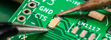
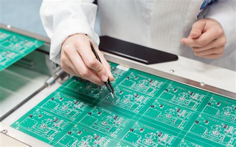
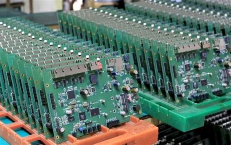
Printed Circuit Boards (PCBs) are the backbone of modern electronics, serving as the foundation for nearly all electronic devices, from smartphones and computers to medical equipment and aerospace systems. Over the decades, PCB technology has evolved significantly, driven by the demand for higher performance, miniaturization, and energy efficiency. As we move further into the 21st century, several key trends are shaping the future of PCB design and manufacturing. This article explores the latest advancements and emerging trends in PCB technology, including high-density interconnects (HDI), flexible and rigid-flex PCBs, additive manufacturing, embedded components, and sustainable practices.
1. High-Density Interconnect (HDI) PCBs
The Push for Miniaturization
As electronic devices become smaller and more powerful, the need for high-density PCBs has grown exponentially. HDI technology enables more components to be packed into a smaller area by utilizing finer traces, microvias, and advanced multilayer stacking techniques.
Key Features of HDI PCBs:
- Microvias: These are extremely small vias (often laser-drilled) that allow for higher connection density.
- Fine-Pitch Components: HDI supports smaller component pitches, enabling compact designs.
- Sequential Lamination: Multiple lamination cycles help achieve complex multilayer structures.
Applications:
- Smartphones and wearables
- Medical implants and diagnostic equipment
- High-performance computing (HPC) and AI hardware
2. Flexible and Rigid-Flex PCBs
The Rise of Bendable Electronics
Flexible PCBs (FPCBs) and rigid-flex PCBs are gaining traction due to their ability to conform to unconventional shapes and withstand mechanical stress.
Advantages:
- Space Efficiency: Eliminates the need for connectors, reducing overall size.
- Durability: Can endure bending, folding, and vibration better than rigid PCBs.
- Lightweight: Ideal for aerospace and portable electronics.
Emerging Applications:
- Foldable smartphones and rollable displays
- Wearable health monitors
- Automotive electronics (e.g., curved dashboards)

3. Additive Manufacturing and 3D-Printed PCBs
Revolutionizing Prototyping and Low-Volume Production
Traditional PCB manufacturing involves subtractive processes (etching copper layers), but additive manufacturing (3D printing) is emerging as a disruptive alternative.
Benefits of 3D-Printed PCBs:
- Rapid Prototyping: Faster design iterations without expensive tooling.
- Complex Geometries: Enables unconventional PCB shapes.
- Reduced Waste: More environmentally friendly than traditional etching.
Current Limitations:
- Limited material options (conductive inks vs. traditional copper).
- Lower conductivity and durability compared to conventional PCBs.
Future Outlook:
As conductive inks and printing techniques improve, 3D-printed PCBs may become viable for mass production.
4. Embedded Components
Integrating Passive and Active Components
Embedding components within the PCB substrate (rather than surface-mounting) reduces size, improves signal integrity, and enhances reliability.
Types of Embedded Components:
- Passive Components: Resistors, capacitors, and inductors.
- Active Components: ICs and semiconductor dies.
Advantages:
- Improved Electrical Performance: Shorter signal paths reduce latency and EMI.
- Enhanced Thermal Management: Better heat dissipation.
- Higher Reliability: Fewer solder joints mean fewer failure points.
Applications:
- High-frequency RF and 5G devices
- Automotive radar and LiDAR systems
- Military and aerospace electronics
5. Advanced Materials for Next-Gen PCBs
Beyond FR-4: New Substrates for High-Performance Applications
Traditional FR-4 laminates are being supplemented (or replaced) by advanced materials to meet the demands of high-speed and high-frequency applications.
Emerging PCB Materials:
- High-Frequency Laminates (e.g., Rogers, Teflon): For 5G and mmWave applications.
- Thermally Conductive Substrates: For power electronics and LED lighting.
- Ceramic-Based PCBs: For extreme environments (high temperature, high power).
Impact on PCB Design:
- Better signal integrity at higher frequencies.
- Improved thermal management for power-dense designs.
6. Sustainable and Eco-Friendly PCB Manufacturing
The Green PCB Movement
With increasing environmental regulations, PCB manufacturers are adopting sustainable practices.
Key Initiatives:
- Lead-Free and Halogen-Free Materials: Reducing toxic substances.
- Recycling and Waste Reduction: Recovering precious metals from discarded PCBs.
- Energy-Efficient Manufacturing: Using renewable energy sources in production.
Challenges:
- Higher costs for eco-friendly materials.
- Performance trade-offs in some green alternatives.
Future Outlook:
Biodegradable PCBs and circular economy models may become mainstream.
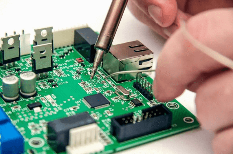
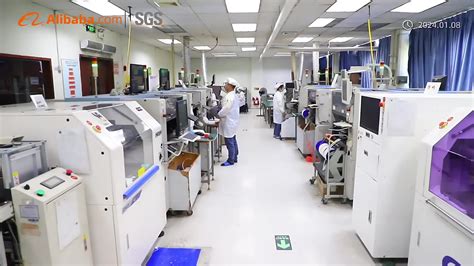
7. AI and Automation in PCB Design & Manufacturing
Smart Factories and AI-Driven Design
Artificial Intelligence (AI) and automation are transforming PCB production.
Applications:
- AI-Powered Design Tools: Optimizing layouts for signal integrity and thermal performance.
- Automated Optical Inspection (AOI): Enhancing defect detection.
- Robotic Assembly: Increasing precision and reducing human error.
Benefits:
- Faster time-to-market.
- Lower production costs.
- Higher consistency in quality.
Conclusion
The PCB industry is undergoing a transformative phase, driven by innovations in materials, manufacturing techniques, and design methodologies. Key trends such as HDI, flexible PCBs, additive manufacturing, embedded components, and sustainability are shaping the future of electronics. As AI and automation further optimize production, PCBs will continue to evolve, enabling next-generation technologies like IoT, 5G, and quantum computing. Staying ahead of these trends will be crucial for engineers, manufacturers, and businesses aiming to lead in the competitive electronics market.
The future of PCB technology is not just about making circuits smaller and faster—it’s about making them smarter, more adaptable, and environmentally responsible.