The Impact of PCB Vias and Effective Solutions to Mitigate Their Effects
Introduction
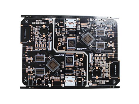
Printed Circuit Boards (PCBs) are the backbone of modern electronics, providing the necessary interconnections between components in increasingly complex electronic devices. Among the various elements that make up a PCB, vias play a critical role in creating three-dimensional connectivity between different layers of the board. However, these essential features can also introduce significant challenges to PCB performance, particularly in high-frequency and high-speed digital applications. This article explores the various impacts of PCB vias on circuit performance and presents comprehensive solutions to mitigate these effects, ensuring optimal signal integrity and power distribution in modern electronic designs.
Understanding PCB Vias
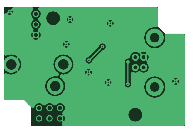
Definition and Types of Vias
Vias are conductive pathways that connect different layers of a PCB, allowing signals and power to traverse between the board’s layers. There are several types of vias commonly used in PCB design:
- Through-hole vias: These extend through the entire thickness of the PCB, connecting all layers.
- Blind vias: These connect an outer layer to one or more inner layers but do not go through the entire board.
- Buried vias: These connect inner layers without reaching either outer surface of the PCB.
- Microvias: These are small-diameter vias (typically less than 150μm) often used in high-density interconnect (HDI) designs.
The Manufacturing Process
Via formation typically involves drilling (mechanical or laser), plating (electroless copper followed by electroplating), and filling (with conductive or non-conductive materials). Each step in this process can introduce variations that affect the via’s electrical characteristics and reliability.
The Impact of PCB Vias on Circuit Performance
Signal Integrity Issues
- Impedance Discontinuities: Vias create impedance mismatches along transmission lines, causing signal reflections that degrade signal quality. The impedance change occurs due to the via’s geometry differing from the trace it connects.
- Insertion Loss: The additional path length and changes in geometry increase insertion loss, particularly at high frequencies where skin effect becomes significant.
- Return Path Discontinuities: Vias can interrupt the reference plane continuity, forcing return currents to find alternative paths that may introduce noise and crosstalk.
- Resonance Effects: Stub portions of vias (unused sections) can act as resonant structures, creating notches in the frequency response.
Power Integrity Challenges
- Increased Inductance: Vias in power distribution networks add parasitic inductance, which can compromise decoupling effectiveness and lead to power supply noise.
- Voltage Drop: The resistance of vias in high-current paths can cause undesirable voltage drops.
- Thermal Issues: Vias can create thermal bottlenecks, especially when they’re the primary path for heat dissipation from inner layers.
Manufacturing and Reliability Concerns
- Plating Quality: Inconsistent plating thickness can lead to reliability issues or increased resistance.
- Thermal Stress: Differences in thermal expansion coefficients between materials can cause via cracking during thermal cycling.
- Filling Challenges: Improperly filled vias may trap chemicals or create voids that affect performance and reliability.
Comprehensive Solutions to Mitigate Via Effects
Design-Level Solutions
- Via Optimization Techniques:
- Via sizing: Use appropriate via diameters; smaller vias have lower capacitance but higher resistance.
- Anti-pad sizing: Optimize clearance holes in reference planes to control capacitance.
- Via stitching: Use multiple vias in parallel for critical connections to reduce inductance.
- Advanced Via Structures:
- Back-drilling: Remove unused via portions (stubs) that cause resonance.
- Via-in-pad: Place vias directly in component pads to minimize loop area (requires filling and planarization).
- Tented vias: Cover vias with solder mask to prevent solder wicking.
- Stackup Design Considerations:
- Arrange signal layers adjacent to their reference planes to minimize via stub length.
- Use symmetrical stackups to balance stresses and reduce warpage.
Material and Process Solutions
- Advanced PCB Materials:
- Use low-loss dielectric materials to mitigate high-frequency losses.
- Consider materials with matched thermal expansion coefficients to reduce stress.
- Improved Manufacturing Processes:
- Laser drilling for more precise via formation, especially for microvias.
- Pulse plating for more uniform copper deposition in high aspect ratio vias.
- Conductive via filling to improve current carrying capacity and thermal performance.
- Surface Finishes:
- Select appropriate finishes (ENIG, immersion silver, etc.) that don’t degrade via performance.
Simulation and Analysis Techniques
- 3D Electromagnetic Simulation:
- Use tools like HFSS or CST to model via behavior in the actual board environment.
- Perform parametric studies to optimize via geometry.
- Signal Integrity Analysis:
- Include via models in channel simulations to assess their impact on eye diagrams.
- Analyze return paths to ensure continuity around vias.
- Power Integrity Simulation:
- Model via inductance in power distribution networks.
- Simulate decoupling effectiveness considering via impedance.
Special Considerations for High-Speed Designs
- Differential Pair Routing:
- Maintain symmetry in via placement for differential pairs.
- Use via coupling techniques to preserve differential impedance.
- High-Speed Design Rules:
- Implement length matching that accounts for via delays.
- Follow manufacturer recommendations for via transitions in high-speed interfaces.
- RF and Microwave Techniques:
- Use via fences to create waveguide-like structures for shielding.
- Implement grounded coplanar waveguide transitions at vias.
Emerging Technologies and Future Trends
- 3D Printed Electronics:
- Additive manufacturing techniques enabling novel via structures.
- Possibility of graded material transitions at via interfaces.
- Advanced Packaging Integration:
- Embedded components reducing the need for some via transitions.
- Silicon interposers with through-silicon vias (TSVs) for high-density interconnects.
- Machine Learning in Via Design:
- AI-assisted via placement and optimization.
- Predictive models for via reliability based on manufacturing data.
- Quantum Computing Applications:
- Specialized via requirements for cryogenic PCB operation.
- Superconducting via materials and structures.
Conclusion
PCB vias, while essential for multilayer board functionality, introduce numerous challenges that can compromise signal integrity, power distribution, and overall system reliability. The effects range from impedance discontinuities and resonance problems in high-speed signals to increased inductance in power delivery networks and various manufacturing reliability concerns.
However, through careful design practices, material selection, advanced manufacturing techniques, and comprehensive simulation analysis, these challenges can be effectively mitigated. Designers must consider via effects early in the design process and implement appropriate solutions tailored to their specific application requirements, whether working with high-speed digital, RF, or power electronics.
As PCB technology continues to evolve with higher frequencies, greater densities, and more demanding applications, via management remains a critical aspect of successful board design. The ongoing development of new materials, manufacturing processes, and design tools promises to further improve our ability to control and optimize via performance in future electronic systems.
By understanding the comprehensive impact of vias and implementing the solutions discussed, engineers can ensure their PCB designs meet the rigorous performance and reliability requirements of modern electronics while pushing the boundaries of what’s possible in electronic packaging and interconnection technology.