The Real Problem with PCB Autorouters
Recently years that self-driving cars were introduced to the public, rockets were re-landed from space with fine-tuned precision for reuse, and Moore’s Law continued on its endless trajectory of growth. However, one thing missing from all of these technological advances is a good autorouter.
The Real Problem with Autorouters
Although PCB autorouters have been around for as long as engineers have known CAD, the implementation of automated technology has been almost completely ignored by engineers involved in designing dense boards. And no wonder. Autorouting algorithms have barely changed since their initial introduction.
Combine stagnant technology with EDA vendors offering autorouting technology at varying levels of performance and configuration, and it’s no wonder that autorouters haven’t been able to keep up. The technology that could save design time and enhance workflow has not made substantial progress to match the expertise and efficiency of an experienced PCB engineer. Is that really all an autorouter needs to offer?
Early Autorouting Technology
The first autorouters produced by EDA vendors had poor results and performance. Most of these routers did not provide guidance or configuration for signal integrity and often added too many vias to the process. Other issues with the early technology included the fact that autorouters were limited to a strict X/Y grid with skew between layers.
Due to these limitations, board space was often wasted and engineers were left to clean up the mess of an uneven board layout. Engineers often spent more time fixing a poor layout caused by the autorouters than they would have spent manually routing. From the beginning, autorouting was off to a bad start.
Over time, autorouting technology improved only slightly and fell far short of the expectations of PCB engineers. Problems continued to exist with poorly spaced board layouts, skewed layers, and too many vias. To move this problematic technology forward, EDA vendors began to adopt new component and board technologies that made it easier to meet signal integrity requirements.
If there is one way to characterize the advancement of autorouting technology in today’s era, it is that hardware limitations have become a hindrance. Without the aid of a dedicated CPU and additional memory to support the required data, autorouters algorithms could not reduce the grid size to provide better routing quality. In the absence of a hardware-based solution, EDA vendors began to explore other approaches, including shape-based autorouting.
These new shape-based autorouters did meet the requirements of board manufacturing and signal integrity by:
Making effective connections between components
Using fewer vias during the autorouting process, thereby reducing PCB costs
Using fewer layers on the PCB while increasing spacing
Despite these advances, autorouting technology remained objectively mediocre. Although EDA vendors overcame hardware limitations, PCB engineers were still skeptical about adopting autorouting technology.
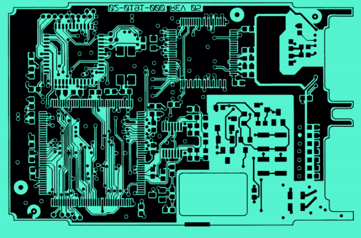
Labyrinth Autorouting Example[2]
Low-Progress in the 1990s
Understanding the impact of the new millennium, autorouters continued to improve with new features, including optimizing angles, pushing routing patterns, using fewer vias, and even glossing techniques to remove extra wire segments. In addition, there were also autorouting techniques to eliminate any layer deviations.
While all these new advances sound extremely promising, have they had the necessary impact on the PCB design community? Unfortunately, no. The more EDA vendors forced autorouting technology onto reluctant PCB designers, the more side effects occurred, including:
Increased board yields with incomplete and poorly routed circuits.
Increased complexity of autorouting configurations, requiring expert configuration.
PCB designers spend more time fixing poor autorouting paths.
The 90s saw a continuing trend – manual routing was still king when the design was near completion.
Shape-based autorouting
Will the 00s bring new hope?
The millennium arrived, bringing new components and board technologies that changed the way PCBs were manually routed. Via counts were now required to be reduced in most designs to maintain signal integrity. Signals began to require delay/timing management, differential pairs began to become the standard for high-speed applications, and BGAs became the preferred choice for many larger pin count packages. These changes in design awareness gave rise to the era of River-Routing.
Rivernet routing is surprisingly efficient and significantly reduces the number of vias on the board, uses all layers evenly, and has no routing layer bias. Despite these advances, it has been rarely adopted. Why? This time it’s not because of the technology, but because of the habits of PCB designers. Because PCB designers are constantly simulating the routing of the board in their minds during the process of placing components, which directly affects how/where parts are placed, which in turn affects the routing implementation. For many engineers, trying to interrupt the middle of this workflow with rivernet routing is not feasible.
As an alternative to rivernet routing, a new trend has emerged in route planning. This method provides designers with a complete toolset to configure autorouting settings, including layer stack definition, design rule constraints, signal shielding, etc. All of these settings are to ensure that automatic routing can be achieved, but configuring properties still takes more time than the manual routing process.
Different paths to the same destination – same goal, different methods
Despite all these advances in autorouting technology over the past three decades, it is still rarely adopted by most engineers. Is it the problem with the technology itself, or is there a conflict between the expectations of PCB designers and autorouters?
Specifically, PCB engineers collaborate on component placement and routing, often identifying logical component placement and interconnection points in a 10,000-foot view of the board layout. Autorouters, on the other hand, tackle this same routing problem from the bottom up, one interconnect at a time.
For denser board layouts, engineers often sketch bus systems and subsystems on paper and use them as a guide for the manual routing process. Engineers often consider several other variables as they place components, including delivery dates, design complexity, product cost, and more.
And of course, there is the dreaded Engineering Change Order (ECO). ECOs can trigger a nightmarish chain reaction, especially when they affect complex design sections, such as BGAs. For these types of tasks, autorouters are only effective tools if they can optimize trace escape or fanout without adding extra vias. Although good designers can reduce the problems of this process by optimizing pin assignments, the problem still exists, with or without an autorouter.
What the EDA Industry Really Needs
Thirty years later, we are still waiting for an interactive router that can instantly transform a desired routing topology into reality with a single click. What does future autorouting technology need to include to be taken seriously?
Agility. The technology needs to be flexible enough to give PCB designers full control over routing direction, location, and selection, regardless of design complexity.
Efficiency. The technology takes less time to route and is more efficient than manual routing.
Simplicity. The technology needs to be easily configurable, allowing PCB designers to edit paths as needed.
Quality. The technology needs to maintain signal integrity quality while routing and distributing paths across multiple layers, without layer bias.
Reliability. The technology needs to consistently produce reliable results that are manufacturing-ready on the first try.
Integration. The technology needs to integrate with our existing designs and tie into our design constraints.
Affordability. To be widely used, it needs to be affordable to all PCB designers.