The Role of PCB Current and Its Importance in Electronic Devices
Introduction
Printed Circuit Boards (PCBs) are the backbone of modern electronic devices, providing mechanical support and electrical connections for various components. One of the most critical aspects of PCB design is managing electrical current, as it directly impacts performance, reliability, and safety. This article explores the fundamentals of PCB current, its effects on electronic devices, and best practices for optimizing current flow in PCB design.
1. Understanding Current in PCBs
1.1 What is Electric Current?
Electric current refers to the flow of electrons through a conductor, measured in amperes (A). In a PCB, current flows through copper traces that connect different components, such as resistors, capacitors, and integrated circuits (ICs).
1.2 Types of Current in PCBs
- Direct Current (DC): Most PCBs use DC, where current flows in a single direction (e.g., from a battery or power supply).
- Alternating Current (AC): Some high-frequency PCBs (e.g., RF circuits) may experience AC effects, requiring impedance matching and signal integrity considerations.
1.3 Factors Affecting PCB Current
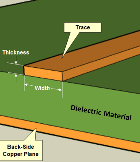
- Trace Width and Thickness: Wider and thicker traces handle higher currents with less resistance.
- Copper Weight: Measured in ounces per square foot (e.g., 1 oz, 2 oz), higher copper weight reduces resistance.
- Temperature Rise: Excessive current can cause overheating, leading to thermal stress and failure.
- Current Density: High current density (A/mm²) can lead to electromigration, degrading traces over time.
2. The Role of PCB Current in Electronic Devices
2.1 Power Distribution
PCBs distribute power from sources (e.g., batteries, power supplies) to components. Proper current management ensures stable voltage levels and prevents voltage drops.
2.2 Signal Integrity
High-speed digital and analog circuits require controlled current flow to minimize noise, crosstalk, and signal distortion. Impedance matching and proper grounding are essential.
2.3 Thermal Management
Excessive current generates heat, which can damage components. PCBs must be designed with thermal vias, heat sinks, and proper trace widths to dissipate heat efficiently.
2.4 Reliability and Longevity
Overloaded traces can lead to failures such as:
- Trace Burnout: Excessive current melts copper traces.
- Electromigration: Metal atoms migrate due to high current density, causing open circuits.
- Delamination: Overheating weakens PCB material bonds.
3. PCB Design Considerations for Optimal Current Flow
3.1 Trace Width Calculation
The width of PCB traces must be sufficient to handle the expected current without excessive heating. The IPC-2221 standard provides guidelines for calculating trace width based on current and temperature rise.
Example Calculation:
For a 1 oz copper PCB carrying 3A with a 10°C temperature rise, the required trace width is approximately 0.7 mm.
3.2 Via Current Capacity
Vias connect different PCB layers and must handle current without excessive resistance. Multiple vias or larger via diameters improve current capacity.
3.3 Ground and Power Planes
- Solid Ground Planes: Reduce impedance and improve current return paths.
- Split Power Planes: Used in mixed-signal designs to prevent noise interference.
3.4 Current Carrying Components
- Fuses and PTCs: Protect against overcurrent conditions.
- Current Sensors: Monitor real-time current flow for safety.
4. Common PCB Current-Related Issues and Solutions
4.1 Voltage Drop
Problem: Long, thin traces cause significant IR drops, leading to insufficient voltage at components.
Solution: Use wider traces or thicker copper layers.
4.2 Electromagnetic Interference (EMI)
Problem: High-current traces can radiate EMI, affecting nearby circuits.
Solution: Implement proper shielding, grounding, and differential signaling.
4.3 Thermal Stress
Problem: High current leads to localized heating, warping the PCB.
Solution: Use thermal relief pads, heat sinks, and proper ventilation.
5. Advanced PCB Current Management Techniques
5.1 High-Current PCB Design
- Bus Bars: Thick metal strips for high-power applications.
- Multilayer PCBs: Distribute current across multiple layers.
5.2 Simulation and Testing
- Finite Element Analysis (FEA): Simulates thermal and current distribution.
- Current Probes and Thermal Imaging: Verify real-world performance.
6. Future Trends in PCB Current Handling
- Higher Power Density: With miniaturization, PCBs must handle more current in smaller spaces.
- Advanced Materials: Graphene and ceramic substrates improve thermal and electrical performance.
- AI-Optimized Designs: Machine learning helps optimize trace layouts for current efficiency.
Conclusion
PCB current management is crucial for the performance, reliability, and safety of electronic devices. By understanding current flow, optimizing trace design, and implementing thermal management strategies, engineers can ensure efficient and long-lasting PCBs. As technology advances, innovative materials and design techniques will further enhance PCB current handling capabilities, enabling more powerful and compact electronic systems.


