Thin film ceramic pcb
Advantages Of Thin Film Ceramic PCB In High-Frequency Applications
Thin film ceramic printed circuit boards (PCBs) have emerged as a pivotal technology in high-frequency applications, offering a multitude of advantages that make them indispensable in various advanced electronic systems.
These advantages stem from their unique material properties, manufacturing precision, and performance characteristics, which collectively contribute to their growing adoption in industries such as telecommunications, aerospace, and medical devices.
One of the primary advantages of thin film ceramic PCBs is their exceptional thermal conductivity.
Unlike traditional PCB materials such as FR4, ceramics like alumina and aluminum nitride can efficiently dissipate heat generated by high-frequency components. This thermal management capability is crucial in preventing overheating and ensuring the reliability and longevity of electronic devices operating at high frequencies. Consequently, thin film ceramic PCBs are particularly well-suited for applications where thermal performance is a critical concern.
In addition to superior thermal properties, thin film ceramic PCBs exhibit excellent electrical insulation.
The high dielectric strength of ceramic materials minimizes the risk of electrical breakdown, even under high voltage conditions. This characteristic is especially important in high-frequency applications, where maintaining signal integrity and preventing cross-talk between adjacent traces are paramount. The inherent electrical insulation properties of ceramics thus contribute to the overall performance and reliability of the PCB.
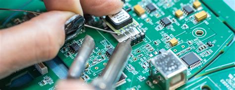
Moreover, the precision manufacturing techniques used in the production of thin film ceramic PCBs enable the creation of intricate and highly accurate circuit patterns.
Advanced photolithography and sputtering processes allow for the deposition of thin metal films with fine line widths and tight tolerances. This level of precision is essential for high-frequency applications, where even minor deviations in circuit geometry can significantly impact performance. The ability to produce highly detailed and consistent circuit patterns ensures that thin film ceramic PCBs can meet the stringent requirements of modern high-frequency electronic systems.
Furthermore, the mechanical robustness of ceramic materials provides an additional layer of reliability.
Ceramics are inherently resistant to mechanical stress, vibration, and environmental factors such as moisture and chemical exposure. This durability makes thin film ceramic PCBs ideal for use in harsh operating environments, where traditional PCB materials might fail. The combination of mechanical strength and environmental resilience ensures that these PCBs can maintain their performance over extended periods, even under challenging conditions.
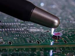
Another notable advantage of thin film ceramic PCBs is their compatibility with a wide range of surface mount devices (SMDs) and integrated circuits (ICs).
The smooth and stable surface of ceramic substrates facilitates the reliable attachment of components, reducing the risk of solder joint failures and enhancing overall assembly quality. This compatibility is particularly beneficial in high-frequency applications, where the precise placement and secure attachment of components are critical to achieving optimal performance.
In conclusion, the advantages of thin film ceramic PCBs in high-frequency applications are manifold.
Their superior thermal conductivity, excellent electrical insulation, precision manufacturing capabilities, mechanical robustness, and compatibility with advanced components collectively make them an ideal choice for demanding electronic systems. As the demand for high-frequency applications continues to grow, the adoption of thin film ceramic PCBs is likely to expand, driven by their ability to meet the stringent performance and reliability requirements of modern technology.
Manufacturing Process Of Thin Film Ceramic PCB
The manufacturing process of thin film ceramic PCBs is a sophisticated and intricate procedure that involves several precise steps to ensure the production of high-quality, reliable circuit boards.
Thin film ceramic PCBs are highly valued in various industries, including aerospace, medical devices, and telecommunications, due to their excellent thermal stability, high-frequency performance, and superior mechanical strength.
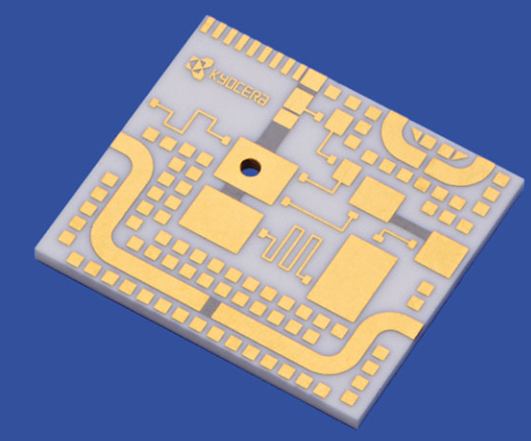
The process begins with the selection of the ceramic substrate, typically made from materials such as alumina (Al2O3), aluminum nitride (AlN), or beryllium oxide (BeO). These materials are chosen for their exceptional thermal conductivity and electrical insulation properties, which are crucial for the performance of the final product.
Once the substrate material is selected, it undergoes a thorough cleaning process to remove any contaminants that could affect the adhesion of the thin film layers.
This cleaning process often involves ultrasonic cleaning, chemical etching, and plasma cleaning to ensure the substrate surface is pristine. Following the cleaning, a thin film of metal, usually gold, platinum, or a combination of metals, is deposited onto the ceramic substrate using a technique called sputtering. Sputtering involves bombarding a target material with high-energy particles, causing atoms to be ejected and deposited onto the substrate in a thin, uniform layer.
After the initial metal layer is deposited, the next step is to define the circuit pattern.
This is achieved through photolithography, a process that uses light to transfer a geometric pattern from a photomask to a light-sensitive photoresist layer applied on top of the metal film. The photoresist is then developed, revealing the desired circuit pattern. The exposed metal areas are subsequently etched away using a chemical etchant, leaving behind the precise circuit design on the ceramic substrate.
To enhance the performance and reliability of the thin film ceramic PCB, additional layers of dielectric materials and metals may be added.
This multilayer construction is achieved through repeated cycles of sputtering, photolithography, and etching. Each layer is carefully aligned and bonded to ensure proper electrical connectivity and mechanical integrity. The dielectric layers, often made from materials such as silicon dioxide (SiO2) or silicon nitride (Si3N4), provide insulation between the metal layers and help to control the electrical properties of the circuit.
Once the multilayer structure is complete, the thin film ceramic PCB undergoes a series of rigorous testing and inspection procedures to ensure it meets the required specifications and performance standards. These tests may include electrical testing to verify circuit continuity and resistance, thermal cycling to assess the board’s ability to withstand temperature fluctuations, and mechanical testing to evaluate its durability and strength.
In conclusion, the manufacturing process of thin film ceramic PCBs is a highly specialized and meticulous procedure that involves multiple steps, including substrate preparation, thin film deposition, photolithography, etching, and multilayer construction. Each step is critical to achieving the desired performance characteristics and ensuring the reliability of the final product. The use of advanced materials and precise manufacturing techniques makes thin film ceramic PCBs an essential component in high-performance applications across various industries.
Thermal Management Solutions Using Thin Film Ceramic PCB
Thin film ceramic PCBs have emerged as a pivotal solution in the realm of thermal management, particularly in high-performance electronic applications. These advanced substrates offer a unique combination of thermal conductivity, electrical insulation, and mechanical stability, making them indispensable in industries where efficient heat dissipation is critical. As electronic devices continue to shrink in size while increasing in power density, the need for effective thermal management solutions has never been more pressing. Thin film ceramic PCBs address this challenge by providing a robust platform that can handle the thermal loads generated by modern electronic components.
One of the primary advantages of thin film ceramic PCBs is their exceptional thermal conductivity.
Unlike traditional FR4 substrates, which are limited in their ability to dissipate heat, ceramic materials such as aluminum oxide (Al2O3) and aluminum nitride (AlN) offer significantly higher thermal conductivity. This property ensures that heat generated by electronic components is efficiently transferred away from the source, thereby reducing the risk of overheating and enhancing the overall reliability of the device. Moreover, the high thermal conductivity of ceramic substrates allows for more compact designs, as the need for bulky heat sinks and other cooling mechanisms is minimized.
In addition to their thermal properties, thin film ceramic PCBs also provide excellent electrical insulation.
This is particularly important in high-voltage applications where electrical isolation between different components is crucial. The inherent dielectric strength of ceramic materials ensures that there is minimal risk of electrical breakdown, even under high operating voltages. Furthermore, the thin film deposition process used in the fabrication of these PCBs allows for precise control over the thickness and uniformity of the insulating layers, resulting in consistent and reliable performance.
Mechanical stability is another key attribute of thin film ceramic PCBs.
Ceramic materials are inherently rigid and resistant to deformation, which makes them ideal for use in environments subject to mechanical stress and vibration. This robustness ensures that the PCB maintains its structural integrity over time, thereby extending the lifespan of the electronic device. Additionally, the thermal expansion coefficient of ceramic substrates is closely matched to that of silicon, which helps to mitigate the risk of thermal stress and delamination during temperature cycling.
The integration of thin film technology further enhances the performance of ceramic PCBs.
Thin film processes, such as sputtering and chemical vapor deposition, enable the deposition of highly uniform and precise conductive traces on the ceramic substrate. This results in improved signal integrity and reduced electrical losses, which are critical for high-frequency and high-speed applications. Moreover, the ability to create fine-pitch interconnects and complex circuit patterns opens up new possibilities for miniaturization and integration in advanced electronic systems.
In conclusion, thin film ceramic PCBs represent a significant advancement in thermal management solutions for modern electronics. Their superior thermal conductivity, electrical insulation, and mechanical stability make them an ideal choice for high-performance applications where efficient heat dissipation and reliability are paramount. As the demand for more powerful and compact electronic devices continues to grow, the adoption of thin film ceramic PCBs is likely to become increasingly widespread, driving further innovation and development in this critical area of technology.
Innovations In Thin Film Ceramic PCB Technology
Thin film ceramic printed circuit boards (PCBs) represent a significant advancement in the field of electronic component manufacturing, offering a range of benefits that make them highly desirable for various high-performance applications. These innovations in thin film ceramic PCB technology are driven by the need for miniaturization, enhanced thermal management, and superior electrical performance, which are critical in sectors such as aerospace, medical devices, and telecommunications.
One of the primary advantages of thin film ceramic PCBs is their exceptional thermal conductivity.
Traditional PCBs, typically made from materials like FR4, often struggle with heat dissipation, which can lead to performance degradation and reduced lifespan of electronic components. In contrast, ceramic substrates, such as aluminum oxide (Al2O3) and aluminum nitride (AlN), offer significantly higher thermal conductivity. This property ensures efficient heat dissipation, thereby maintaining the integrity and reliability of the electronic components mounted on the PCB.
Moreover, thin film ceramic PCBs exhibit excellent electrical insulation properties.
The dielectric strength of ceramic materials is substantially higher than that of conventional PCB materials. This characteristic is particularly beneficial in high-voltage applications where electrical isolation is paramount. Additionally, the low dielectric constant of ceramics minimizes signal loss and crosstalk, which is crucial for maintaining signal integrity in high-frequency circuits.
The miniaturization of electronic devices is another area where thin film ceramic PCB technology excels.
The ability to fabricate fine lines and spaces with high precision is a hallmark of thin film technology. This capability allows for the creation of highly dense circuit patterns, enabling the development of compact and lightweight electronic devices without compromising performance. The use of advanced photolithography techniques in the manufacturing process ensures that even the most intricate designs can be accurately reproduced on the ceramic substrate.
Furthermore, the mechanical robustness of ceramic materials provides an added layer of reliability.
Ceramics are inherently resistant to wear, corrosion, and chemical degradation, making them suitable for use in harsh environments. This durability ensures that thin film ceramic PCBs can withstand the rigors of demanding applications, such as those found in aerospace and industrial automation, where exposure to extreme temperatures and corrosive substances is common.
In addition to these inherent material advantages, recent innovations in thin film ceramic PCB technology have focused on improving the manufacturing processes and material compositions. For instance, advancements in sputtering and chemical vapor deposition (CVD) techniques have enabled the deposition of ultra-thin conductive and dielectric layers with exceptional uniformity and adhesion. These improvements have led to enhanced performance characteristics and greater design flexibility, allowing engineers to push the boundaries of what is possible with thin film ceramic PCBs.
Moreover, the integration of advanced materials, such as graphene and other nanomaterials, into the thin film layers has opened new avenues for enhancing the electrical and thermal properties of ceramic PCBs.
These materials offer unique properties, such as high electron mobility and superior thermal conductivity, which can be leveraged to further improve the performance of electronic devices.
In conclusion, the innovations in thin film ceramic PCB technology are transforming the landscape of electronic component manufacturing.
The superior thermal management, electrical insulation, miniaturization capabilities, and mechanical robustness of ceramic substrates make them an ideal choice for high-performance applications. As manufacturing techniques and material compositions continue to evolve, the potential for thin film ceramic PCBs to drive advancements in various industries remains vast and promising.