Types and selections of PCB surface molding
When making board specifications, the following items should be taken into consideration: PCB substrate material, solder mask, screen printing, surface molding, board size and thickness, copper thickness, blind and buried vias, through-hole plating, SMT, panels, tolerances, etc. should be considered before actually manufacturing the circuit board. Among these items, the choice of surface molding belongs to the first category, because surface molding plays an extremely important role in improving the reliability of electronic products. Since the copper layer on the PCB is easily oxidized, the resulting copper oxide layer will seriously reduce the quality of welding, thereby reducing the reliability and effectiveness of the final product. Surface molding is conductive, which prevents oxidation of the pads and ensures excellent solderability and electrical performance.
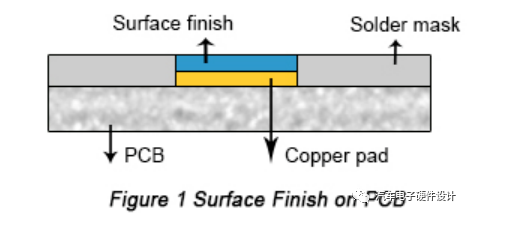
Surface molding or surface coating is the most important step in the process between PCB board manufacturing and circuit card assembly, and has two main functions, one of which is to retain the exposed copper circuit, and the other is to provide a solderable surface when soldering components to the PCB. As shown in Figure 1, the surface molding is located on the outermost layer of the PCB and on top of the copper, playing the role of a “coating” for the copper.
Types of surface forming
Basically, there are two main types of surface forming: metallic and organic. HASL, ENIG/ENEPIG, immersion gold and immersion tin all belong to metallic surface forming, while OSP and carbon ink all belong to organic surface forming.
•HASL (Hot Air Solder Leveling)
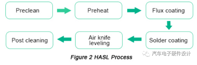
HASL is a traditional surface finishing method applied to PCBs. PCBs are usually immersed in molten solder so that all exposed copper surfaces are covered with solder. Excess solder is removed by passing the PCB between hot air knives. Usually, HASL follows the process shown in Figure 2 below:
In order to comply with regulations on environmental protection, HASL is divided into two subcategories: leaded HASL and lead-free HASL. The latter complies with the RoHS (Restriction of Hazardous Substances) regulations and laws initially adopted by the European Union.
•ENIG and ENEPIG
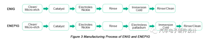
ENIG is short for chemical nickel plating and consists of a thin layer of chemically plated nickel and immersion gold to protect the nickel from oxidation. ENEPIG, also known as chemical nickel chemical palladium gold plating, differs from ENIG in that the palladium layer acts as a resistance layer to block the oxidation and diffusion of nickel into the copper layer. Compared to other types of surface formation, ENIG and ENEPIG provide the highest solderability for PCBs, but at a much higher cost. The difference between the manufacturing process of ENIG and ENEPIG can be found in Figure 3 below.
The chemical nickel step is an autocatalytic process that involves depositing nickel on a copper surface catalyzed by palladium. A reducing agent containing nickel ions must be supplemented to provide the appropriate concentration, temperature, and acidity required to produce a uniform coating. In the immersion gold step, gold adheres to the nickel-plated area through molecular exchange, which will protect the nickel until the soldering process. The thickness of the gold needs to meet certain tolerances to ensure that the nickel maintains its solderability.
ENIG and ENEPIG have their own advantages and disadvantages respectively. For example, ENIG has a flat surface, simple process mechanism and high temperature resistance, while ENEPIG has excellent multiple reflow cycle capability and highly reliable wire bonding capability. According to the comparison between ENIG and ENEPIG, they can be applied in different applications to achieve different purposes. ENIG is suitable for lead-free soldering, SMT (surface mount technology), BGA (ball grid array) packaging, etc. While ENEPIG is able to meet the strict requirements of a variety of packaging including THT (through hole technology), SMT, BGA, wire bonding, press-fit, etc.
•ImAg (Immersion Silver)
ImAg consists of a thin immersion silver plating layer on a copper wire. Generally, ImAg follows the following steps:

ImAg surface forming advantages ImAg surface forming disadvantages
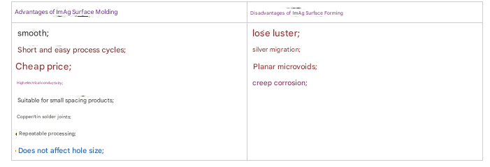
ImAg is a good surface forming type for soldering and testing. Creep corrosion is its main disadvantage.
•ImSn (Immersion Tin)
ImSn is basically the same as ImAg, except that tin is used in ImSn and silver is used in ImAg. In terms of the advantages of ImSn, it provides an extremely flat surface forming on the copper pad, making it very suitable for SMT applications. In addition, ImSn also provides a surface that can be easily detected by common automatic optical inspection technology.
•OSP (Organic Solderability Preservative)
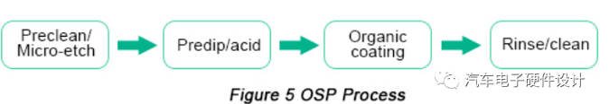
OSP is a surface molding that involves transparent organic materials. It uses a water-based organic compound that selectively binds to copper and protects the copper until soldering. Generally, OSP follows the following process:
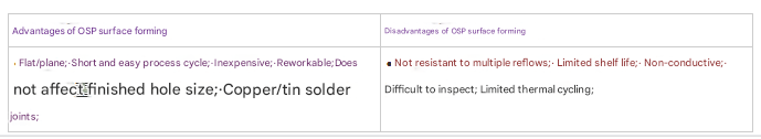
The above description cannot explain anything about OSP. You can refer to the article about OSP that you barely know for more details on OSP surface molding technology.
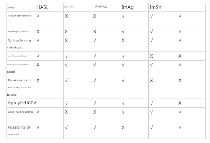
In summary, each type has its own advantages and disadvantages. You should choose the most appropriate surface molding based on the purpose of use of the electronic product, performance requirements, cost, corrosion resistance, ICT (In-Circuit Test), hole filling, etc. The more items considered in the selection process, the higher the accuracy.
Generally speaking, in terms of cost, comparing these types of surface molding, ImAg and OSP are the cheapest, while ENIG is the most expensive. In terms of corrosion resistance, HASL and ImSn have the best corrosion resistance, while ImAg has the worst corrosion resistance. In terms of ICT, only OSP is the worst, while the other OSPs are equally good. In terms of void filling, HASL and ENIG are better than other types.
Surface molding selection
The surface molding selection of PCB is the most important step in PCB manufacturing, because it directly affects the process yield, the number of rework, the field failure rate, the testing capability, the scrap rate, and the cost. All important considerations about assembly must be incorporated into the selection of surface molding to ensure the high quality and high performance of the final product.
In the PCB assembly process, people in different positions have different views on how to choose surface molding, as shown in the figure below:
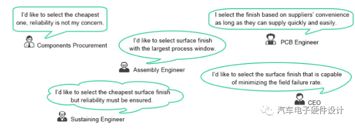
Obviously, people in different positions have different selection criteria. No matter which type is selected, it only meets people’s needs and convenience, and rarely considers the quality, performance and reliability of PCBs and PCB components.
According to the introduction of each type of surface molding above, certain attributes are the most important selection criteria. The following table shows the “have” and “don’t have” attributes of each type of surface molding. According to the specific requirements and functions of the PCB product, you can follow this table to select the ideal surface molding option.
In summary, for the type of surface molding selection, the best type must be selected and numerous functions can be achieved. Each type of surface forming has its own advantages and disadvantages. But don’t worry. There are some engineering tricks to solve the problems caused by surface forming. For example, for the disadvantage of low wetting force of OSP, there are some solutions such as changing the solderability plating of the board or the wave soldering alloy, increasing the top side preheating, etc. The key point is that all possible elements must be considered in order. Get the ideal performance.
Nowadays, environmental issues are becoming more and more important in the field of electronics. In order to limit the harmful substances produced, the European Union has issued RoHS. RoHS, also known as lead-free, stands for Restriction of Hazardous Substances. RoHS, also known as Directive 2002/95/EC, originated from the European Union and restricts the use of six harmful substances found in electrical and electronic products. Since July 1, 2006, all products applicable in the EU market must be RoHS certified. RoHS affects the entire electronics industry as well as many electrical products. Therefore, surface forming of lead-free solder will have more followers in the future.
Comparison between ENIG and ENEPIG
Among the technologies applied in the PCB manufacturing process, those that contribute to surface molding play a vital role in the application of PCB assembly and electronic products in which the circuit board is applied.
The copper layer on the PCB is easily oxidized in the air, which is prone to copper oxidation, which will seriously reduce the soldering quality. However, surface molding is able to prevent the copper pad from oxidizing, so it can guarantee excellent solderability and corresponding electrical performance. The growing market demand for miniaturization, higher functionality and reliability of electronic devices pushes PCBs towards thinness, lightness, high density and higher signal transmission speed. Therefore, surface molding must accept the upcoming challenges in terms of stability and reliability to be compatible with the above development requirements.
In addition, based on the increasing awareness of environmentally friendly sustainable development, environmental pollution issues involving PCB surface molding are increasingly attracting global attention. The RoHS (Restriction of Hazardous Substances) and WEEE (Waste Electrical and Electronic Equipment) regulations formulated by the European Union are aimed at eliminating harmful substances such as lead and mercury in electronic products, requiring the end of green or lead-free PCB surface production. ENIG (Electroless Nickel Immersion Gold) and ENEPIG (Electroless Nickel Immersion Gold) as a kind of surface molding can not only meet the technical requirements required by the PCB market, but also adjust to the trend of lead-free solder, so it has development potential.
However, it is difficult for people to tell the difference between ENIG and ENEPIG, let alone know when to rely on which one. The following content of this article will provide the definition of ENIG and ENEPIG and their manufacturing processes, discuss their advantages and disadvantages, with the aim of providing a guide for when to use each molding in a specific situation.
Surface molding selection considerations
So far, the recognized main surface moldings are HASL (hot air solder leveling), OSP (organic solder preservative), immersion tin, immersion gold, ENIG and ENEPIG. Faced with different surface moldings with their own advantages and disadvantages, have you suffered severe pain when you choose a type that is compatible with your product? In fact, no matter what your PCB product type is or what requirements must be met, your choice of surface molding must be based on cost, application environment of the final product, fine pitch components, lead-free or lead-free, and considerations in RF applications. (high frequency possibility), shelf life, shock and drop resistance, thermal resistance, volume and yield.
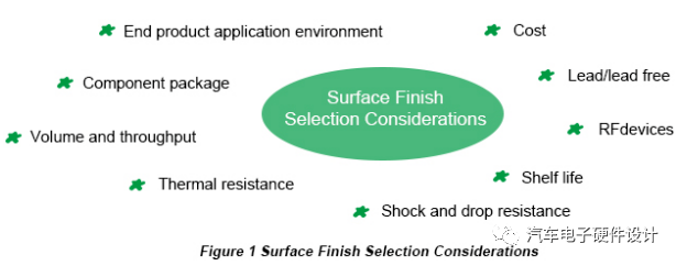
Therefore, the above-mentioned consideration elements can be one of the references for your final decision on PCB surface molding. Of course, these items can never be of average importance with equal importance. Then, before you are ready to rely on this list and consider your specific product situation, the degree of importance of each item should be clarified.
The emergence of ENIG and ENEPIG
As early as the 1990s, due to the development of PCBs towards better lines and microvias, coupled with the prominent shortcomings of HASL and OSP, such as the flatness problem of the former and the flux elimination problem of the latter, ENIG began to be used as another alternative for surface finishing in PCB manufacturing.
In order to defeat black nickel plate, the main weakness of ENIG, ENEPIG came out as an upgraded version of ENIG. By adding palladium plating between chemical nickel and immersion gold, ENEPIG contains a thin layer of resistance, the thickness of which is usually in the range of 0.05μm to 0.1μm. The palladium layer plays a role in preventing the immersion gold technology from corroding the nickel layer. As a result, ENEPIG is able to overcome the defects of black pads held by ENIG. In addition, ENEPIG has highly reliable wire bonding capabilities, excellent multiple reflow soldering capabilities, and the characteristics of containing switch contact surfaces, enabling it to simultaneously meet the stringent requirements of high-density PCBs and multi-surface packaging. Based on these advantages, ENEPIG is also known as universal surface molding.
Advantages and Disadvantages of ENIG and ENEPIG
In the 1990s, with the trend of eliminating micropores and flatness problems of PCB fine lines and HASL (hot air solder leveling) and OSP (organic solderability preservative) to eliminate solder problems, ENIG technology began to be widely used in PCB manufacturing.
Compared with ENIG, ENEPIG technology was applied to PCB manufacturing as early as the 1980s. However, due to the high cost of ENEPIG and the low surface molding requirements of the product, it has not been widely used and promoted. At present, the requirements for miniaturization, thinness, and multi-functions provide more opportunities for ENEPIG.
The following table shows the advantages of ENIG and ENEPIG.
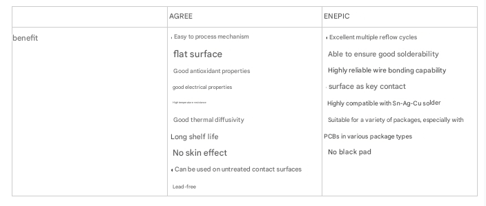
ENEPIG technology is developed on the basis of ENIG technology, in which a palladium layer is added, so its performance is greatly improved. The reason is: a. The palladium layer with a dense film structure is completely covered on the nickel layer, and the phosphorus content in the palladium layer is lower than the ordinary content in the nickel layer, thereby avoiding the conditions for the generation of black nickel and eliminating the possibility of black pads. b. The melting point of palladium is 1,554℃, which is higher than the melting point of gold (1,063℃). Therefore, palladium melts relatively slowly at high temperatures and has enough time to produce a resistance layer for protecting the nickel layer. c. Palladium has a higher hardness than gold, which improves solder reliability, wire bonding capability, and friction reduction. d. Tin-palladium alloy has the strongest anti-corrosion ability and is able to stop creep corrosion caused by primary battery corrosion, which can extend service life. e. The use of palladium is able to reduce the thickness of the gold layer, reducing its cost by 60% compared to ENIG.
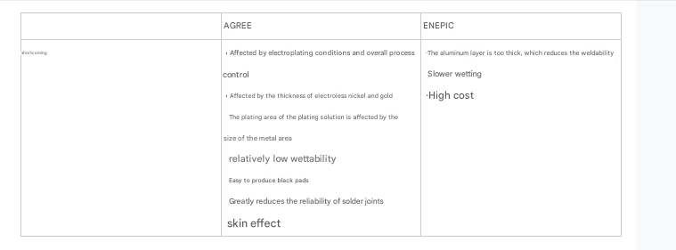
Every coin has two sides. In addition to the advantages, ENIG and ENEPIG also have some disadvantages.
Measures for cost-effective surface forming
Based on the advantages and disadvantages of ENIG and ENEPIG, it is natural to choose ENEPIG as a better solution when reliability is considered first. However, its higher cost prevents some companies from sacrificing some revenue. However, since we have taken measures to eliminate the black pad problem of applying ENIG, you can completely get the best balance between quality and cost.
Black pads were born with the advent of ENIG. In the process of immersing gold into ENIG, black pads are easily caused due to nickel corrosion under poor operation. Excessive nickel corrosion will greatly reduce wettability and reduce soldering performance. When the solder is bonded to the corroded nickel surface, the solder must withstand greater stress. Eventually, the contact layer for contact between solder and nickel will break and produce a black nickel surface, called a black pad.
Since ENIG contains a chemical gold plating layer, it is difficult to conclude whether there is a black pad. Unless the gold is stripped off the surface by chemical methods, the nickel will not be exposed. In addition, a P-rich nickel layer will be formed at the contact of nickel and gold (before soldering) and at the contact of solder and nickel (after soldering). This is actually a natural phenomenon and has nothing to do with the black pad.
There are two main reasons for the black pad. First, the technical implementation is subject to such poor control that the crystal particles grow unevenly and many cracks occur between the crystal particles with low-quality nickel films. Second, it takes a long time to implement gold immersion, so that corrosion is easily generated on the nickel surface and cracks are generated.
Among all the elements that affect chemical nickel plating, the solder mask layer stands out for the following reasons:
Reason 1: The cross-bonding and insufficient rigidity of the solder mask layer easily leave contaminants on the copper surface, thereby preventing the occurrence of the activation reaction. In the hot chemical nickel solution, hydrogen gas is generated to release the solder mask monomer. It then prohibits the reaction of chemical nickel and destroys the chemical balance.
Reason 2: The poor surface of the solder mask will cause the pad surface to deteriorate.
Reason 3: The solder mask filled in the micro-via tends to undergo an electrochemical reaction, which will prevent the formation of a uniform catalytic surface.
To successfully solve the black pad problem, three measures can be taken:
Measure 1: The pH value of the chemical nickel solution should be controlled.
Measure 2: The stabilizer content of the chemical nickel solution must be analyzed.
Measure 3: Nickel surface corrosion should be stopped during immersion gold.
So far, the improvement of immersion gold technology has achieved good results. The newly developed immersion gold technology can not only reduce the corrosion of the nickel surface, but also help reduce costs. Compared with the previous generation of immersion gold solution (pH = 4.5-5.5), the new generation of immersion gold solution has a pH range of 7.0 to 7.2, which is close to neutral. Neutral liquid performs best in stopping hydrogen ions from corroding the nickel surface. Moreover, the new generation of immersion gold technology can be implemented in a lower gold solution, which reduces the cost of the initial raw materials by 50% to 80% and has little effect on the underlying nickel.
When it comes to the surface forming of flexible PCBs, if the current ENIG is applied directly to the flexible circuit board, the nickel film with the layer will produce cracks as the substrate bends, which will further cause cracks in the underlying copper. In order to adapt to the surface forming requirements of flexible boards, the newly developed chemical nickel plating technology is able to produce a nickel film with a columnar structure. When the substrate is bent, only microcracks can be formed on the surface, and the cracks will not spread to the underlying copper.
All the analyses and measures listed above are only applicable to ENIG, and they are not required for ENEPIG as an upgraded version of ENIG.
In fact, the above measures are accumulated and tested by PCB manufacturers to meet customers’ needs for high reliability and low cost. Once ENIG is selected, even if there are “serious” defects due to our customer-oriented principle, we still have the responsibility to ensure its quality.
Application Comparison between ENIG and ENEPIG
The application fields of ENIG and ENEPIG are different due to their unique advantages. ENIG is suitable for lead-free soldering, SMT (surface mount technology), BGA (ball grid array) packaging, etc. The industries and products that ENIG can provide include data/telecom, high-end consumer, aerospace, military and high-performance equipment and medical industries. In addition, due to its high reliability, ENIG is particularly suitable for the flexible market.
ENEPIG is able to meet the more stringent requirements of a variety of packages, including THT (through-hole technology), SMT, BGA, wire bonding, press fit, etc. Even better, ENEPIG is also suitable for PCBs with different packaging technologies. Therefore, the application field of ENEPIG can serve the aerospace, military and high-performance equipment and medical industries that have higher requirements for density and reliability.
In fact, the job of PCB board manufacturers is to provide customers with the best quality products. As an important step in the PCB manufacturing process, high-quality surface molding absolutely determines the high quality of the circuit board. Therefore, PCB manufacturers must ensure that the surface molding can meet the requirements required by the circuit boards and final products they serve.
Technology and Manufacturing Process
It may be a bit dull to understand the technology and manufacturing process of ENIG and ENEPIG, but it allows you to know exactly what will happen with these two surface moldings.
1) Technology and manufacturing process of ENIG
A three-layer metal structure is involved in ENIG, including copper, nickel and gold. The process mainly includes: copper activation, ENP (electroless nickel plating) and immersion gold.
•Copper activation
Copper activation is a privilege for selective deposition in ENP. A displacement reaction is required so that a thin layer of palladium can be generated on the copper layer that acts as a catalytic surface. In the PCB manufacturing process, PdSO4 and PdCl2 are usually used as activators with the following reaction formula:
Cu+Pd2+→Cu2++Pd
•ENP
In ENIG technology, the nickel layer has two functions. As a barrier layer, it can prevent the mutual diffusion of copper and gold. On the other hand, it reacts with tin to generate excellent IMC (intermetallic compound) Ni3Sn4, which can ensure good assembly solderability. Under the action of the catalytic surface, ENP leads to the deposition of the nickel layer through a redox reaction with NaH2PO2 as a reducing agent. Once the nickel layer is completely covered by the palladium catalytic surface, the elemental nickel allows the nickel deposition to continue as a catalyst for ENP.
It is important to point out that the atomic active hydrogen NaH2PO2 emitted by the hydrolysis of the reducing agent reduces Ni2+ to the elemental state of NiH2PO2- and the elemental state of phosphorus. Therefore, the ENP layer in the ENIG technology is actually a nickel-phosphorus alloy layer. The reaction formula of this step is as follows:
ħ2PO2-+ H2O→H^++ HPO32-+ 2H
Ni2++ 2H→Ni↓+ 2H+
ħ2PO2-+ H→P↓+ OH-+ H2ö
ħ2PO2-+ H2O→H^2↑+ H++ HPO32-
- Immersion Gold
In the ENIG technology, the advantages of the gold layer are low contact resistance, less oxidation opportunity, high strength and anti-friction, which can meet the circuit conductivity requirements and protect the copper layer and the nickel layer from oxidation, thereby ensuring the solderability of the nickel layer. Immersion gold refers to the generation of a gold layer on the surface of the nickel layer through a replacement reaction, and the replacement reaction will not stop until the generated gold layer is completely covered by the nickel layer. This is why the gold layer is relatively thin. The reaction formula indicating this step is as follows:
2AU(CN)2+Ni→2AU +Ni2++ 4CN-
2) ENEPIG Technology and Manufacturing Process
Unlike ENIG, ENEPIG adopts a four-layer metal structure, including copper, nickel, palladium and gold. The process of ENEPIG is the same as that of ENIG, except that chemical palladium plating is added between ENP and immersion gold.
The palladium layer is added to the ENEPIG technology as a barrier layer, which prevents the corrosion of the nickel layer caused by the solution during the process of gold deposition and diffusion from the nickel layer to the gold layer. At the same time, due to the compactness of the palladium layer to increase solderability, it can be used as an anti-oxidation layer and an anti-corrosion layer. Similar to chemical nickel plating, chemical palladium plating leads to the deposition of a palladium layer through a redox reaction with NaH2PO2 as a reducing agent. The reaction formula indicating this step is as follows:
ħ2PO2-+ H2O→H^++ HPO32-+ 2H
Pd2++ 2H→Pd↓+ 2H+
ħ2PO2-+ H→H↓+ OH-+ H2ö
ħ2PO2-+ H2O→H^2↑+ H++ HPO32-