Understanding PCB Assembly Drawings for Effective Design
Key Takeaways
Understanding PCB assembly drawings is crucial for optimizing the design and assembly process of printed circuit boards (PCBs). These drawings serve as the blueprint for manufacturers, detailing every aspect of the assembly, from placement of components to connections. Key components include a precise layout of the board, which illustrates component placement, solder pads, and other necessary features for fabrication. Moreover, symbols and notations utilized in pcb assembly drawings are pivotal for conveying important information that ensures accuracy during assembly.
Incorporating best practices, such as maintaining clarity in PCBA documentation and ensuring adherence to industry standards, significantly improves the efficiency of the design process. Techniques like utilizing clear visual aids and providing detailed instructions contribute to fewer errors and a smoother assembly workflow.
Below is a table summarizing some key aspects that enhance understanding of PCB assembly:
| Aspect | Description |
|---|---|
| Component Layout | Arrangement of components on the PCB for optimal function |
| Soldering Techniques | Methods used to ensure reliable connections between components |
| Testing Procedures | Strategies to confirm that all assemblies function correctly |
| Documentation Standards | Guidelines ensuring consistency in PCB documentation |
In conclusion, mastering these takeaways allows designers and assemblers to navigate common challenges effectively while paving the way for successful outcomes in PCBA projects.
Introduction to PCB Assembly Drawings
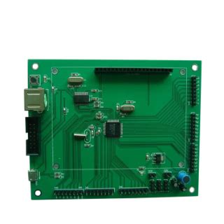
Printed Circuit Boards (PCBs) are the backbone of modern electronics, and understanding PCB assembly drawings is crucial for anyone involved in the design and manufacturing process. These drawings serve as a map, providing detailed information on how components are to be placed and interconnected on the board. A well-constructed PCB assembly drawing will include critical details such as component placement, soldering instructions, and a list of materials. By familiarizing oneself with these elements, engineers can ensure that the assembly process is efficient and error-free.
The role of PCBA (Printed Circuit Board Assembly) cannot be overstated; it transforms an array of components into a functioning electronic device. Effective communication through assembly drawings helps prevent costly mistakes that may arise during production. Following industry standards while creating these drawings allows for clarity and consistency across different teams involved in the manufacturing process.
Moreover, embracing best practices in making these drawings can significantly enhance collaboration among designers and assemblers. “A well-documented PCB assembly drawing is like a recipe; it guides you step by step to achieve the desired outcome,” > suggests an industry expert. Thus, understanding symbols and notations used in PCB assembly drawings can greatly facilitate this process.
Ultimately, proficient use of PCB assembly documentation not only accelerates the physical production but also optimizes testing processes post-assembly. As technology continues to advance, keeping abreast of trends in design methodologies will be vital for success in this ever-evolving field.
Key Components of PCB Assembly Drawings
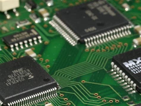
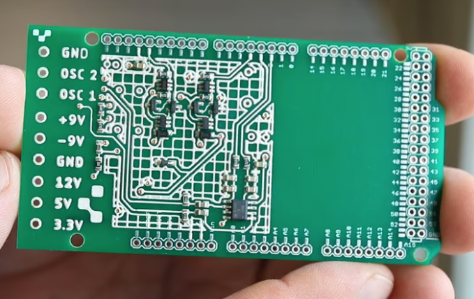
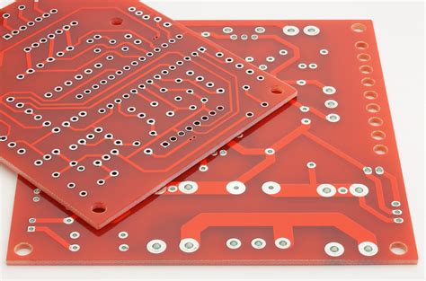
PCB assembly drawings serve as vital documents that facilitate the pcba process, bridging the gap between design and actual assembly. These drawings encompass several key components that are crucial for ensuring a smooth production cycle. First and foremost, a bill of materials (BOM) is included, detailing every component required for assembly, such as resistors, capacitors, and integrated circuits. Each item in the BOM is essential for identifying specific parts during the pcb assembly process.
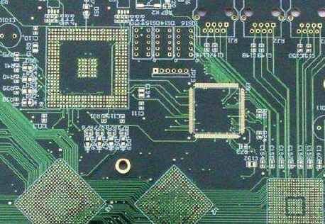
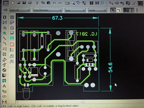
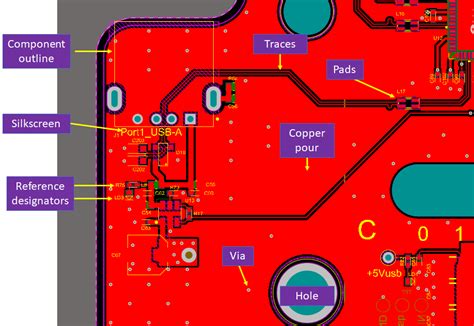
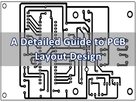
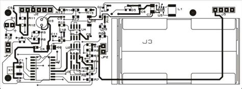
Additionally, the layout representation in PCB assembly drawings is critical. It visually showcases component placements and detailed routing of circuitry. This aids technicians during assembly by providing a clear guideline to follow. Furthermore, any special notations or instructions are embedded in these drawings to convey specific handling or placement techniques that must be observed to ensure optimal performance of the assembled board.
Symbols used in PCB assembly drawings also play a significant role; they provide immediate clarity about connections and component functions. For instance, different shapes may represent various components, while lines indicate electrical connections or specific pathways between elements on the board.
In summary, understanding these critical components within pcb assembly drawings not only enhances the efficiency of the assembly process but also significantly contributes to achieving desired performance outcomes in electronic devices. By applying effective design practices and utilizing standard symbols and notations, engineers can create comprehensive guides that streamline production efforts and ensure high-quality outputs.
Understanding Symbols and Notations
A comprehensive understanding of symbols and notations in PCB assembly is crucial for effective design and communication among engineers and manufacturers. These symbols serve as shorthand representations for various components, connections, and attributes that are fundamental to creating a reliable Printed Circuit Board Assembly (PCBA). They encompass a wide array of notations detailing everything from electronic components like resistors and capacitors to connections indicating how these components are linked within the overall layout.
For instance, the use of standardized symbols for common components ensures that designers can quickly ascertain the specifications just by glancing at the assembly drawing. Additionally, notations indicating layer specifications, pad sizes, and drill hole dimensions are vital in ensuring that all parties involved are on the same page regarding how the pcb assembly should be executed. Misinterpretation of these symbols can lead to errors during production, such as incorrect placements or inappropriate soldering techniques—factors that can severely impact performance.
Moreover, understanding these notations helps in translating complex designs into actionable assembly instructions. It enhances collaboration between design engineers and assembly technicians by providing a clear visual guide that minimizes ambiguity. The ability to interpret these symbols accurately fosters smoother workflows in production settings, ultimately leading to more successful outcomes in PCB designs. As technology progresses, adherence to evolving notation standards becomes even more paramount for maintaining compatibility across different platforms in PCBA processes, thereby ensuring the longevity and reliability of electronic products.
Best Practices for Effective PCB Design
Effective PCB design is paramount for ensuring that a printed circuit board assembly (PCBA) performs optimally in its intended application. To achieve this, designers must embrace several best practices that streamline both the design and implementation processes. First and foremost, a thorough understanding of the pcb assembly process is essential. This includes not only recognizing the various components and their placement but also being mindful of how design decisions impact manufacturability. Utilizing standardized symbols and notations in PCB assembly drawings is crucial, as it enhances clarity and reduces errors by providing a common language for designers and manufacturers alike.
Moreover, incorporating proper dimensioning and tolerances in drawing specifications allows for better alignment during assembly. Designers should also prioritize signal integrity by carefully routing traces to minimize interference while ensuring adequate spacing between components to prevent overheating. A well-thought-out layout can significantly ease the PCBA process, reduce manufacturing costs, and improve overall product reliability. Lastly, collaborating closely with manufacturing teams from the early stages of design will provide valuable feedback that can lead to more efficient production practices, culminating in successful outcomes for the final product. The integration of these best practices into routine design procedures ultimately contributes to higher quality assemblies and enhanced performance in deployed applications.
Techniques for Enhanced Assembly Processes
To achieve optimal results in PCB assembly (PCBA), it is crucial to implement a set of effective techniques that streamline the manufacturing process. One of the most important techniques is ensuring precise alignment of components on the printed circuit board. This can be achieved through the use of automated placement machines, which significantly reduce human error and increase efficiency. Additionally, employing solder paste printing with high precision can enhance the reliability of solder joints, resulting in better performance of the assembled product.
Another essential technique is conducting thorough inspections at various stages of assembly. Utilizing automated optical inspection (AOI) systems allows for real-time monitoring and immediate detection of errors or defects in the assembly process. This proactive approach minimizes rework and reduces overall production costs, as faults can be addressed promptly without affecting subsequent stages.
Furthermore, staying updated on the latest materials and technology advancements plays a vital role in enhancing assembly processes. Implementing newer materials that provide better thermal management or are easier to work with can significantly improve product durability and functionality. Incorporating lean manufacturing practices is also beneficial, as it emphasizes waste reduction while maximizing productivity.
Ultimately, utilizing these advanced techniques not only improves the efficiency of PCB assembly but also ensures that quality standards are met consistently, leading to successful outcomes in PCBA projects. By adopting these methodologies, design engineers and manufacturers can foster innovation and enhance overall productivity within their operations.
Common Challenges in PCB Assembly
When it comes to PCB assembly, several challenges can hinder the overall effectiveness of the process. One prevalent issue is component placement errors, which can occur if the placement of individual components on the printed circuit board does not align accurately with the design specifications. This misalignment not only affects the functionality of the pcba but can also lead to costly rework or even complete failure of the final product. Another significant challenge is dealing with soldering defects, such as insufficient solder or cold solder joints, which can compromise connections and reliability. Managing these issues requires an understanding of best practices in the assembly process, along with using modern techniques and tools for inspecting and verifying assembly quality. Additionally, thermal management during assembly presents another layer of complexity; excessive heat during soldering can damage sensitive components, necessitating careful control and monitoring. With advancements in technology and effective design practices, however, many of these challenges can be mitigated, leading to more successful PCB designs and assemblies that meet performance expectations.
Case Studies: Successful PCB Designs and Assemblies
The landscape of PCB assembly and its effective practices is vividly illustrated through various case studies that highlight successful designs and assemblies. One noteworthy example includes a leading consumer electronics company that adopted an innovative approach to PCBA. By integrating advanced design software, they were able to streamline the layout process, reducing the time spent on revisions significantly. This not only improved the assembly efficiency but also enhanced the overall product performance. Another intriguing case involves a medical device manufacturer that utilized collaborative techniques between engineering teams and assembly operators, which led to a remarkable decrease in production errors. This synergy allowed for real-time feedback during PCB assembly, resulting in a superior quality assurance process. Through these examples, it becomes apparent that effective communication among all stakeholders, along with a comprehensive understanding of PCB assembly drawings, is pivotal in achieving optimal results in any project. Furthermore, these success stories underline the significance of embracing modern technology and adopting best practices that can lead to increased reliability and functionality in PCBA. As we analyze these cases, it is clear that a thoughtful approach to design and assembly not only meets but exceeds industry standards, paving the way for future innovations in electronics manufacturing.
Future Trends in PCB Design and Assembly Drawings
The realm of PCB assembly and the associated drawings is evolving rapidly, driven by technological advancements and the increasing demands of the electronics market. As we look ahead, several key trends are shaping the future of PCBA practices. Firstly, the rise of automation and robotics in pcb assembly processes is optimizing efficiency and precision, leading to a reduction in human error while expediting production timelines. Additionally, advancements in design software are enabling more intuitive interfaces and enhanced simulations, allowing designers to visualize their creations with greater accuracy before physical prototypes are made. This evolution encourages a stronger collaboration between hardware and software engineers to optimize designs for manufacturability. Furthermore, the integration of sustainable practices in PCB design is becoming more prominent; eco-friendly materials and processes are gaining traction as industries seek to minimize their environmental footprint. The push for miniaturization of electronic components also continues to influence pcb assembly, demanding more intricate designs that can fit into smaller devices without compromising functionality. As these trends emerge, companies that stay informed and adapt their strategies will likely achieve significant advantages in developing innovative products that resonate with consumer needs while ensuring reliable manufacturing practices.
Conclusion
In summary, understanding PCB assembly drawings is crucial for anyone involved in the design and manufacturing of printed circuit boards. These drawings serve as a vital communication tool that encapsulates the technical specifications and assembly requirements, making it easier for engineers and technicians to collaborate effectively. By mastering the essential components of PCBA documentation, such as layout views, component placement, and assembly notes, teams can identify potential issues before production begins, leading to a more streamlined process. Furthermore, familiarizing oneself with industry-standard symbols and notations can significantly enhance the clarity of pcb assembly instructions. Emphasizing best practices and adopting proven techniques can mitigate common pitfalls in assembly processes, ultimately resulting in successful outcomes. With continuous advancements in technology and design methodologies, staying informed about emerging trends will ensure that professionals remain at the forefront of PCB assembly innovation for years to come.
FAQs
What is a PCB assembly drawing?
A PCB assembly drawing is a detailed illustration that represents the component layout and the assembly process of a printed circuit board (PCB). It provides critical information needed to effectively assemble the PCB, ensuring all components are correctly positioned.
Why are PCB assembly drawings important?
PCB assembly drawings are essential as they serve as a roadmap for the manufacturing process. They help in minimizing errors, optimizing assembly time, and ensuring that all parts are correctly placed. A well-structured PCBA facilitates efficient production and leads to improved product quality.
What components are typically included in PCB assembly drawings?
Typically, PCB assembly drawings include information such as component references, placement locations, and soldering specifications. These components ensure that assemblers have all the necessary details to perform the assembly accurately.
What symbols should I look for in PCB assembly drawings?
In PCB assembly drawings, you will encounter various symbols that denote electrical characteristics and component types. Understanding these symbols helps in interpreting the drawing accurately and executing the pcba process without complications.
How can I ensure effective design practices with my PCB assemblies?
To ensure effective design practices, always follow best practices such as using standardized symbols and clear notations in your drawings. Additionally, collaboration with engineers during the design stage can help highlight potential issues early on.
For more detailed information on pcb assembly, please visit our site.