Understanding PCB Current: Design Considerations and Best Practices
Introduction to PCB Current
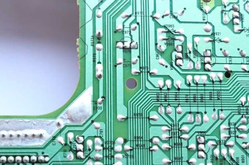
Printed Circuit Board (PCB) current refers to the flow of electrical charge through the conductive traces and planes of a PCB. Proper management of current flow is fundamental to PCB design, affecting everything from basic functionality to long-term reliability. Current handling capacity determines trace widths, via sizes, layer stackup, and overall thermal performance of the board.
In modern electronics, PCBs must handle currents ranging from microamps in signal lines to hundreds of amps in power electronics. Understanding how current behaves in PCB conductors and how to properly design for various current requirements separates successful designs from those that fail prematurely.
Fundamental Concepts of Current Flow in PCBs
Ohm’s Law and Current Density
At its core, current flow in PCBs follows Ohm’s Law (V=IR), where the voltage drop (V) across a conductor equals the current (I) multiplied by the resistance (R). The resistance of PCB traces depends on:
- Conductor material (typically copper)
- Cross-sectional area (width × thickness)
- Length of the trace
- Temperature (resistance increases with temperature)
Current density (J), measured in A/mm² or A/mil², represents the amount of current per unit area of conductor. High current densities lead to excessive heating and potential reliability issues.
Skin Effect at High Frequencies
For high-frequency signals (typically above 10 MHz), the skin effect causes current to flow primarily near the surface of conductors rather than uniformly throughout the cross-section. This effectively reduces the usable cross-sectional area, increasing AC resistance. The skin depth (δ) is given by:
δ = √(ρ/(πfμ))
Where:
- ρ = resistivity of the conductor
- f = frequency
- μ = permeability of the conductor
This phenomenon becomes particularly important in RF designs and high-speed digital circuits.
Proximity Effect
When parallel conductors carry alternating currents, the proximity effect causes current to concentrate on the sides of conductors facing each other. This further increases AC resistance beyond what the skin effect alone would cause.
PCB Current Capacity Considerations
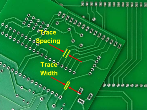
Trace Width Calculations
Determining appropriate trace widths is crucial for current handling. Several methods exist:
1. IPC-2152 Standard
The most authoritative reference is IPC-2152 (“Standard for Determining Current-Carrying Capacity in Printed Board Design”), which provides comprehensive guidelines based on empirical data. It considers:
- Current magnitude
- Allowable temperature rise
- Copper weight (thickness)
- Board material
- Presence of nearby traces or planes
- Internal vs. external layers
2. Simplified Formulas
For quick estimates, designers often use modified versions of the old IPC-2221 formulas:
For external traces:
I = k × ΔT^0.44 × A^0.725
For internal traces:
I = k × ΔT^0.44 × A^0.725 × 0.8
Where:
- I = current (A)
- ΔT = temperature rise (°C)
- A = cross-sectional area (mil²)
- k = 0.048 for external, 0.024 for internal
3. Online Calculators
Numerous online tools implement IPC-2152 calculations, allowing designers to input parameters and receive recommended trace widths.
Copper Weight and Thickness
PCB copper thickness is specified in ounces per square foot (oz/ft²), representing the thickness if 1 oz of copper were spread over 1 ft² area. Common weights include:
- 0.5 oz (17.5 μm)
- 1 oz (35 μm)
- 2 oz (70 μm)
- 3 oz (105 μm)
- 4 oz (140 μm)
Heavier copper allows higher current capacity or narrower traces but increases cost and affects impedance control.
Temperature Rise Considerations
The allowable temperature rise (ΔT) significantly impacts current capacity. Common design targets:
- 10°C rise: Conservative design for high reliability
- 20°C rise: Typical general-purpose design
- 30-50°C rise: For cost-sensitive or space-constrained designs
Higher temperature rises reduce required trace widths but increase operating temperatures, potentially affecting component lifetimes and long-term reliability.
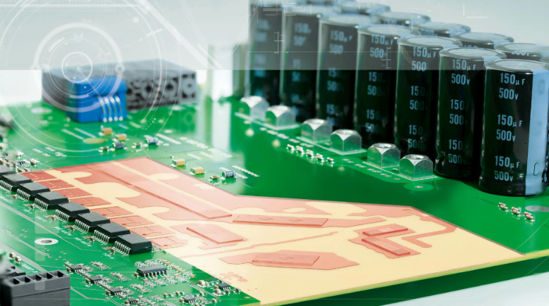
High Current PCB Design Techniques
Power Planes
For high current applications, dedicated power planes offer several advantages over traces:
- Lower resistance due to large cross-sectional area
- Better heat dissipation
- Reduced inductance
- Improved power distribution
Multiple Layers for Current Sharing
When single layers cannot handle required currents, designers can:
- Use multiple layers connected with vias
- Implement parallel traces on the same layer
- Combine both approaches
Proper via placement is critical to ensure current divides evenly between layers.
Via Current Capacity
Vias have limited current capacity due to their small cross-section and potential for uneven plating. Considerations include:
- Via diameter (larger is better)
- Barrel plating thickness
- Number of parallel vias
- Thermal relief connections
As a rough guideline, a standard 0.3mm via with 25μm plating can handle about 1A, but this varies significantly with design parameters.
Bus Bars and Embedded Conductors
For extremely high currents (50A+), traditional PCB conductors may be insufficient. Solutions include:
- Soldered or bolted bus bars
- Embedded copper rods or bars
- Heavy copper PCBs (up to 20 oz)
- Hybrid designs combining PCB and wire conductors
Thermal Management for High Current PCBs
Heat Dissipation Strategies
High currents generate heat through I²R losses. Effective heat dissipation methods include:
- Thermal vias under hot components
- Increased copper area (pours, planes)
- External heatsinks
- Board edge connectors for heat transfer
- Strategic component placement for airflow
Thermal Expansion Considerations
Different coefficients of thermal expansion (CTE) between copper and substrate materials can cause mechanical stress during temperature cycling. Design techniques to mitigate:
- Avoid sharp corners in high-current traces
- Use curved or tear-drop transitions
- Consider flex areas for high-expansion regions
Current Measurement and Testing
PCB Current Measurement Techniques
Verifying current handling requires careful measurement:
- Four-wire Kelvin measurement for accurate resistance
- Thermal imaging to identify hot spots
- Voltage drop measurements along traces
- Destructive testing for qualification
Accelerated Life Testing
High-current PCBs often undergo:
- Temperature cycling
- Current cycling
- Vibration testing
- Long-term burn-in

Special Considerations for Different Applications
Power Electronics
Features:
- Very high currents (tens to hundreds of amps)
- High di/dt requirements
- Significant thermal challenges
- Often use specialized substrates (IMS, ceramic)
Design priorities:
- Minimize loop inductance
- Optimize thermal paths
- Implement current sharing
- Consider creepage and clearance
High-Speed Digital
Features:
- Moderate DC currents but fast transitions
- Careful attention to return paths
- Controlled impedance critical
Design priorities:
- Maintain uninterrupted return paths
- Proper decoupling capacitor placement
- Minimize simultaneous switching noise
- Manage skin and proximity effects
RF and Microwave
Features:
- Skin effect dominates
- Surface roughness affects losses
- Often use specialized materials
Design priorities:
- Wide, thick conductors for low loss
- Careful via transitions
- Impedance control
- Minimal discontinuities
Future Trends in PCB Current Handling
Advanced Materials
Emerging materials promise better current handling:
- Graphene-enhanced conductors
- Superconducting materials (for cryogenic applications)
- Nanostructured copper alloys
3D Printed Electronics
Additive manufacturing enables:
- Non-planar current paths
- Graded conductor cross-sections
- Integrated cooling channels
Active Current Management
Smart PCBs may incorporate:
- Distributed current sensors
- Active thermal management
- Self-healing conductors
Conclusion
Proper PCB current handling requires balancing electrical requirements, thermal management, manufacturability, and cost. By understanding fundamental principles, applying industry standards like IPC-2152, and implementing appropriate design techniques, engineers can create reliable PCBs that meet current-carrying requirements across diverse applications. As electronics continue pushing power density limits, innovative approaches to PCB current management will remain essential for technological progress.
Designers must remember that while calculations provide starting points, real-world conditions often require conservative margins and empirical verification. A thorough approach considering all aspects of current flow—from DC resistance to high-frequency effects—leads to robust, reliable PCB implementations capable of meeting today’s demanding electronic requirements.


