Understanding PCB Design and Assembly for Optimal Results
Key Takeaways
Understanding the intricacies of PCB design and pcb assembly is crucial for anyone working on electronic projects. Successful pcba requires attention to a variety of factors that can significantly influence the performance and reliability of the final product. First and foremost, embracing the key principles established in effective design can help streamline both processes. One should focus on creating a clear schematic and layout, ensuring components are correctly aligned to avoid potential issues during assembly.
Utilizing essential tools and software becomes indispensable when drafting designs or troubleshooting any problems that arise. Modern software often offers simulation capabilities, allowing designers to foresee potential pitfalls before moving to actual production. In terms of assembly, meticulous practices such as maintaining a clean workspace, using quality materials, and adhering strictly to assembly guidelines are vital.
“Invest time in understanding your components; this knowledge will pay off throughout both the design and assembly phases.”
Moreover, nurturing an awareness of current innovations in PCB technology can provide insights into more efficient methods that enhance performance while reducing costs. As trends in the industry evolve, integrating new materials or techniques can keep your projects competitive.
Ultimately, achieving optimal results requires a continuous commitment to learning and adapting within these two domains—designing effective PCBs and executing precise pcb assemblies—ensuring that electronic projects not only meet but exceed expectations.
Introduction to PCB Design and Assembly
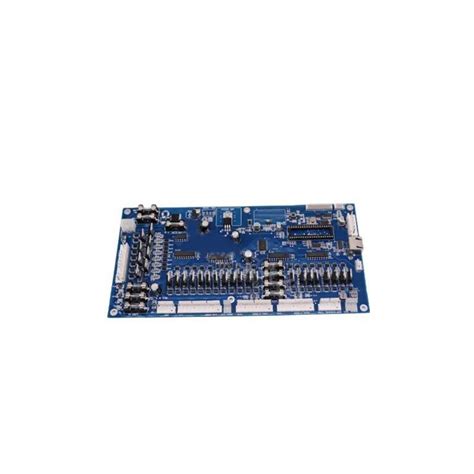
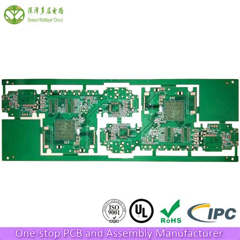
In the world of electronics, understanding PCB design and pcb assembly is fundamental for creating efficient and effective products. A printed circuit board (PCB) serves as the backbone of electronic devices, providing both a physical structure for components and a pathway for electrical connections. The process of designing a PCB involves several critical steps, including schematics creation, layout design, and the selection of appropriate materials. Once the design phase is completed, pcb assembly (often referred to as PCBA) takes center stage. This phase encompasses various processes such as soldering components onto the board and ensuring each connection is reliable.
For successful PCB assembly, attention to detail is paramount; small errors during assembly can lead to significant issues later on. Implementing best practices in both design and assembly can greatly enhance the functionality and durability of the final product. Additionally, innovations in materials and technology are continually reshaping how PCBs are designed and assembled, making it essential for engineers to stay updated with industry trends.
As you venture into your electronic projects, mastering these key aspects of pcb assembly will enable you to achieve optimal results that meet both performance expectations and industry standards. Understanding these foundational elements empowers engineers—whether they are beginners or seasoned professionals—to produce high-quality electronic devices that are reliable and efficient in operation.
Key Principles of Effective PCB Design
Effective PCB design is crucial for the success and performance of any electronic project. To achieve optimal results, it is essential to adhere to several key principles. First and foremost, a clear understanding of the circuit’s functionality and its requirements will guide the layout process. A well-structured schematic diagram serves as the foundation for effective pcb assembly.
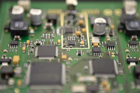
Next, maintaining adequate spacing between components is vital to minimize interference and ensure reliability. Trace width and thickness should be calculated based on current requirements to prevent overheating, while selecting appropriate materials influences the board’s overall performance.
The integration of vias must be strategically planned; they should not disrupt the flow of signals or power transmission. Additionally, implementing good grounding practices will significantly enhance signal integrity and reduce crosstalk within the design.
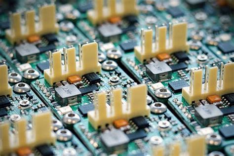
Moreover, proper component placement facilitates easier assembly during pcb assembly processes (PCBA). An organized layout can enhance manufacturability, allowing for automated processes that can save time and reduce errors.
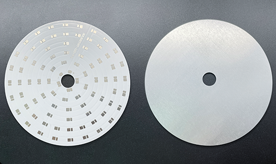
Innovative techniques such as using surface mount technology (SMT) can optimize space on your PCB while improving performance through reduced parasitic effects. Ultimately, adhering to these principles will guide both beginners and experienced designers in creating high-quality PCBs capable of meeting demanding specifications in today’s complex electronic landscape.
Essential Tools and Software for PCB Design
When embarking on a journey into PCB design and assembly, selecting the right tools and software is fundamental to achieving high-quality outcomes. There is a diverse array of software available for PCB design, ranging from entry-level programs to advanced suites used by professional engineers. Popular options include Altium Designer, Eagle, and KiCAD, each offering unique features that cater to different experience levels and project needs. For beginners, user-friendly interfaces and comprehensive tutorials can significantly ease the learning curve, while seasoned professionals might seek more sophisticated functionalities such as simulation capabilities, advanced routing algorithms, or integration with CAD systems.
In addition to design software, having the right tools for pcb assembly is equally crucial. A basic toolkit should include soldering irons, multimeters, and PCB holders. As projects become more complex, investing in reflow ovens for surface-mount technology (SMT) or automated pick-and-place machines can boost efficiency in your PCBA process. Moreover, embracing innovative technologies like 3D printing for rapid prototyping can also greatly enhance your workflow by allowing for quick iterations and modifications.
Ultimately, understanding which tools and software best fit your specific needs will enable you to streamline your design and assembly processes. By merging effective technology with best practices in both PCB design and assembly, you can significantly improve the performance and reliability of your electronic projects.
Best Practices in PCB Assembly
Effective PCB assembly (often referred to as PCBA) is crucial for ensuring the reliability and performance of the final product. To achieve optimal results, several best practices can be followed throughout the assembly process. First and foremost, it is essential to adhere to the manufacturer’s specifications for all components. This not only guarantees compatibility but also minimizes potential errors during assembly.
Additionally, maintaining a clean workspace can significantly affect the outcome of your PCB assembly projects. Contaminants like dust or grease can lead to poor solder joints and ultimately malfunctioning circuits. Employing proper handling techniques, such as using anti-static mats and wrist straps, helps prevent static damage to sensitive components.
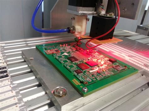
Another best practice involves conducting thorough inspections at various stages of the PCBA process. Pre-assembly checks should confirm that all components match design specifications and that there are no physical defects on the boards themselves. After assembly, visual and automated inspections (like Optical Inspection Systems) can identify common issues, ensuring each pcb assembly meets quality standards.
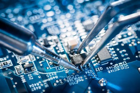
Moreover, using effective soldering techniques is vital in achieving robust connections. The selection of quality solder materials alongside appropriate temperature control during processes such as surface mount technology (SMT) leads to better adhesion and electrical performance.
Finally, documenting each step in the process provides invaluable insight for future projects. It allows for troubleshooting if any issues arise post-production and enhances collective knowledge about successful strategies in PCB design and assembly.
| Best Practices | Description |
|---|---|
| Follow Specifications | Use manufacturer guidelines for all components |
| Clean Workspace | Keep the area free from dust and contaminants |
| Conduct Inspections | Perform checks pre-assembly and post-assembly |
| Soldering Techniques | Use quality solder materials with proper temperature control |
| Documentation | Record each step for reference in future projects |
By integrating these practices into your workflow, you can enhance both efficiency and quality in your pcb assembly, leading to superior electronic devices that perform reliably in diverse applications.
Troubleshooting Common PCB Issues
One of the key challenges faced in PCB design and pcb assembly is the identification and resolution of common issues that may arise during production or operation. Understanding these issues can help in ensuring a more robust outcome in your projects. For example, misalignment of components can lead to performance failures; thus, it’s essential to utilize precise design specifications and assembly techniques. Additionally, the selection of materials significantly affects reliability; poor choices in substrates or solder types can result in heat management issues or insufficient electrical connectivity. Regular inspection during the pcba process is crucial to catching defects early on, as visual inspections combined with automated testing equipment can help to identify solder bridging and component placement errors that would otherwise go unnoticed. Furthermore, employing best practices throughout your PCB design process—including adhering to electrical standards and incorporating redundancy where appropriate—will minimize the potential for these problems. Always bear in mind that good documentation plays a vital role; maintaining comprehensive records of schematics and manufacturing processes aids significantly during troubleshooting efforts. Ultimately, addressing these common issues early on enhances overall quality and ensures optimal performance in your electronic projects.
Innovations in PCB Technology
The world of PCB design and assembly has witnessed remarkable advancements that have transformed traditional approaches into more efficient and innovative methodologies. One significant development is the emergence of flexible PCBs, which allow for designs that can bend and twist, opening new possibilities in compact electronic devices. Additionally, the integration of Internet of Things (IoT) technology into PCBA processes enhances connectivity and functionality, making it easier to embed intelligence in everyday products. Electronic components are also getting smaller and more powerful, leading to high-density interconnects (HDI) that enable manufacturers to pack more functionality into smaller footprints. This shift demands precise assembly techniques and meticulous design practices to ensure reliability in compact spaces. Furthermore, advancements in automated assembly technologies have improved the speed and accuracy of pcb assembly, drastically reducing human errors while increasing productivity. As we continue to embrace these innovations, the focus remains on achieving high-quality results that optimize both performance and manufacturability in electronic projects, ensuring that professionals adapt effectively to these changes in the field. As such, it is crucial for both newcomers and seasoned professionals to stay informed about the latest trends and techniques shaping the future of pcb assembly and overall PCB development.
Future Trends in PCB Design and Assembly
As the landscape of electronics continues to evolve, so too do the trends in PCB design and assembly. One significant trend is the increased adoption of flexible printed circuit boards (FPCBs), which provide enhanced adaptability in a variety of applications, particularly in wearable technology and compact devices. Another notable development is the rise of automated PCB assembly (PCBA) processes, which utilize advanced robotics and artificial intelligence to increase efficiency and reduce human error during production. This not only leads to faster turnaround times but also ensures higher precision in component placement.
Additionally, sustainability is becoming central to both PCB design and assembly practices. Designers are increasingly focused on utilizing eco-friendly materials that minimize waste while maximizing performance. This shift not only caters to consumer demand for greener products but also aligns with global efforts towards reducing environmental impact. Moreover, the integration of IoT (Internet of Things) technologies is transforming traditional pcb assembly practices by enabling smarter manufacturing processes that leverage real-time data analytics for improved quality control.
With these advancements, it is essential for both newcomers and seasoned professionals in the field to stay informed about emerging trends that could shape their projects. Understanding these future trajectories will be vital for achieving optimal results in any electronic endeavor while ensuring that designs remain competitive in a rapidly changing market.
Conclusion: Achieving Optimal Results in Your Projects
In the realm of PCB design and assembly, achieving optimal results is a culmination of various thoughtful practices and attention to detail throughout the process. Whether you are a beginner or a seasoned professional, understanding the significance of pcba quality will significantly impact your project’s success. Applying the key principles of effective design, utilizing essential tools, and refining your techniques in pcb assembly can lead to enhanced functionality and reliability in your electronic products. Furthermore, recognizing potential issues early on can save valuable time and resources. Innovative techniques and advancements in technology promise exciting new possibilities that can elevate your projects. By integrating these insights, you increase your chances of creating functional and successful electronic designs that stand out in today’s competitive landscape. Ultimately, meticulous planning combined with practical experience will enable you to navigate the complexities of pcb design and ensure that both aesthetic and technical requirements are met for optimum performance.
Conclusion: Achieving Optimal Results in Your Projects
In summary, a thorough understanding of PCB design and pcb assembly processes is essential for producing high-quality electronic devices. By combining the best practices of effective PCB design with innovative pcba techniques, engineers can significantly enhance the performance and reliability of their products. Key considerations such as component placement, signal integrity, and thermal management must take precedence during both the design and assembly phases. Recognizing the importance of selecting the right materials and tools is also crucial; these decisions can impact not only functionality but also production costs and timelines. As technology continues to advance, embracing new trends and innovations in PCB technology will enable professionals to stay competitive in an ever-evolving market. Hence, achieving optimal results in your electronic projects requires a holistic approach that integrates both well-designed circuitry and precise assembly methods.
FAQs
What is PCB assembly?
PCB assembly, commonly referred to as PCBA, involves the process of soldering electronic components onto a printed circuit board (PCB). This procedure is vital for creating functional electronics.
What are the steps involved in PCB assembly?
The key steps in PCB assembly include: designing the PCB, fabricating the board, assembling components (either manually or using automated machinery), and then testing the assembled PCB for functionality.
Why is PCB design important?
Effective PCB design is crucial as it determines the performance and reliability of the electronic device. A well-designed circuit board can lead to fewer errors during pcb assembly, thus enhancing overall product quality.
What are some common issues in PCB assembly?
Common issues can include misaligned components, soldering defects, and incorrect component placement. Addressing these issues early in the pcb assembly process can help prevent costly mistakes.
How can I choose a reliable PCB manufacturer?
When selecting a manufacturer for PCBA, consider their certifications, experience, reviews from previous clients, and their capacity to meet your project’s specific needs.
For more insights on pcb assembly, innovative techniques, and to optimize your projects’ success, please visit this link for further information.