Understanding PCB Impedance Mismatch: Causes, Effects, and Mitigation Strategies
Introduction
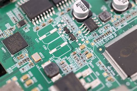
Printed Circuit Boards (PCBs) are the backbone of modern electronics, enabling the interconnection of various components to form complex circuits. As signal frequencies continue to rise—especially in high-speed digital, RF, and microwave applications—maintaining proper impedance control becomes crucial. Impedance mismatch is a common issue in PCB design that can lead to signal integrity problems, including reflections, attenuation, and data corruption.
This article explores the fundamentals of PCB impedance mismatch, its causes, effects on circuit performance, and effective mitigation strategies to ensure optimal signal integrity.
1. What is Impedance Mismatch in PCBs?
Impedance mismatch occurs when the characteristic impedance of a transmission line does not match the impedance of the source, load, or interconnected components. In PCB design, transmission lines (such as microstrips, striplines, and coplanar waveguides) are designed to have a specific characteristic impedance (typically 50Ω or 75Ω for RF applications and 90Ω–100Ω for differential pairs).
When there is a mismatch, part of the signal reflects back towards the source instead of being fully transmitted to the load. This phenomenon is governed by the reflection coefficient (Γ), which is calculated as:
[
\Gamma = \frac{Z_L – Z_0}{Z_L + Z_0}
]
Where:
- ( Z_L ) = Load impedance
- ( Z_0 ) = Characteristic impedance of the transmission line
If ( Z_L = Z_0 ), there is no reflection (( \Gamma = 0 )). However, any deviation causes partial or full reflection, leading to signal degradation.
2. Causes of Impedance Mismatch in PCBs
Several factors contribute to impedance mismatches in PCB designs:
2.1. Improper Trace Geometry
The characteristic impedance of a PCB trace depends on its width, thickness, and the dielectric properties of the substrate. Variations in these parameters—due to manufacturing tolerances or design errors—can alter impedance.
- Trace Width Variations: Narrower traces increase impedance, while wider traces decrease it.
- Dielectric Thickness (H): Thinner dielectrics reduce impedance, while thicker ones increase it.
- Copper Thickness: Thicker copper lowers impedance due to increased capacitance.
2.2. Discontinuities in Transmission Lines
Any abrupt change in the transmission path can cause impedance mismatches, including:
- Vias: Vertical interconnects introduce parasitic inductance and capacitance.
- Bends & Corners: Sharp 90° bends increase capacitance, altering impedance.
- Connectors & SMD Pads: Transition points between traces and components often have impedance variations.
2.3. Material Inconsistencies
- Dielectric Constant (Dk) Variations: Different PCB materials (FR4, Rogers, etc.) have varying Dk values, affecting impedance.
- Resin Content & Weave Pattern: In FR4, the glass weave can cause localized impedance variations.
2.4. Poor Termination Techniques
- Missing or Incorrect Termination Resistors: High-speed signals (e.g., DDR, USB, PCIe) require proper termination to prevent reflections.
- Stub Effects: Unused branches (stubs) in transmission lines act as parasitic elements.
2.5. Frequency-Dependent Effects
At higher frequencies, skin effect and dielectric losses become significant, altering the effective impedance.
3. Effects of Impedance Mismatch
Impedance mismatch leads to several signal integrity issues:
3.1. Signal Reflections
- Ringging & Overshoot: Reflected waves interfere with the original signal, causing oscillations.
- Standing Waves: In RF circuits, mismatches create standing waves, reducing power transfer efficiency.
3.2. Increased Insertion Loss
Mismatches cause energy loss, weakening the signal amplitude at the receiver.
3.3. Data Integrity Issues in High-Speed Digital Circuits
- Jitter & Timing Errors: Reflections introduce uncertainty in signal transitions.
- Bit Errors: In severe cases, data corruption occurs due to distorted waveforms.
3.4. EMI & Crosstalk
Reflected energy can radiate, increasing electromagnetic interference (EMI) and crosstalk in adjacent traces.
4. Mitigation Strategies for Impedance Mismatch
To minimize impedance mismatch, PCB designers employ several techniques:
4.1. Controlled Impedance Design
- Use Impedance Calculators: Tools like Polar SI9000 help determine trace geometry for target impedance.
- Simulate with EM Solvers: Tools like Ansys HFSS or Keysight ADS verify impedance before fabrication.
4.2. Proper Termination Techniques
- Series Termination: Adds a resistor near the driver to match source impedance.
- Parallel Termination: Places a resistor at the load end to absorb reflections.
- AC Termination: Uses an RC network for high-frequency matching.
4.3. Minimizing Discontinuities
- Avoid 90° Bends: Use 45° or curved traces.
- Optimize Via Design: Use back-drilling, blind/buried vias, or via stitching for high-speed signals.
- Reduce Stub Lengths: In differential pairs, keep stubs as short as possible.
4.4. Material Selection
- Low-Dk Materials: For high-frequency designs, use Rogers or other low-loss laminates.
- Consistent Substrate Thickness: Ensure uniform dielectric properties.
4.5. Post-Fabrication Testing
- Time-Domain Reflectometry (TDR): Measures impedance variations along traces.
- Vector Network Analyzer (VNA): Characterizes S-parameters to identify mismatches.
5. Conclusion
Impedance mismatch in PCBs is a critical issue that affects signal integrity, especially in high-speed and RF applications. By understanding its causes—such as trace geometry variations, discontinuities, and material inconsistencies—designers can implement effective mitigation strategies. Techniques like controlled impedance routing, proper termination, and minimizing discontinuities help ensure optimal performance.
As signal speeds continue to increase, adhering to best practices in impedance control will remain essential for reliable PCB designs. Through careful simulation, material selection, and testing, engineers can minimize reflections and maintain signal fidelity in modern electronic systems.


