Using PCB Tolerances to Improve Productivity
Well-defined PCB tolerances are critical to building high-quality boards. Nearly all PCB manufacturing steps are subject to tolerances, many of which you define during the design process. If you work with your contract manufacturer (CM) to select these so that they fall within the tolerances of their equipment and processes, your boards can achieve the best results and achieve the best yield. Before defining how to select the best PCB tolerances, we should clearly define defects and what types will affect our goal of 100% productivity.
How Do Tolerances Impact Productivity?
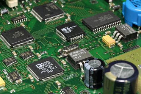
The yield of a fully assembled PCB or PCBA is often associated with building a large number of boards, which in many cases requires the transition from prototype to high-volume production. In other cases; especially specialized designs for critical systems in aerospace, medical devices, and industrial applications, low-volume production is the final stage of manufacturing. Whether it is a low-volume or high-volume, the goal of the final stage of PCBA production is a perfect yield or zero boards with defects that cannot be used as intended.
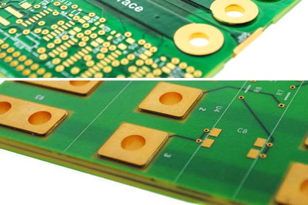
PCB defects that may be the root cause in manufacturing can be mechanical defects. Less obvious things like delamination, bending, or breaking can distort electrical operation; as can contamination or moisture on or within the board. Boards can also become exposed to moisture and contamination after they are assembled. Therefore, it is best to employ PCB moisture protection methods during and after manufacturing. In addition to defects that may not be discovered until the board is assembled and put into service, there are also obvious defects that can render a board unusable.
The number of boards produced divided by the number of usable boards is the yield. The difference is the number of defective boards that require rework (additional actions must be taken to correct small defects and get the board into a usable state). For PCBAs where rework cannot correct defects, a redesign may be necessary. This can mean additional man-hours, as well as increased manufacturing and testing costs.

How PCB Tolerances Improve Yield
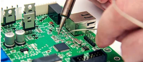
The importance of your choice of assembly service cannot be overstated. Making the right choice can be the difference between receiving a board designed to meet or exceed regulatory standards. IPC classification or not. Likewise, the benefits of DFM for your PCBA development cannot be overstated. Tailoring design decisions within the PCB tolerances of your CM equipment and processes ensures that your board can actually be built. The constraints defined by regulations establish acceptable boundaries for the CM’s DFM tolerance range. The PCB tolerances you select must fall within these ranges.
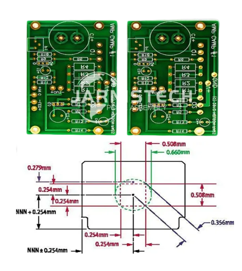
The absolute range of the CM equipment’s capabilities at a particular manufacturing step defines its process window. For example, the absolute minimum diameter of a drilled hole defines the minimum width of the process window for creating a via. Similarly, the maximum hole width defines the maximum process window width for creating a via. As long as these physical dimensions all meet regulatory requirements, you are free to choose any dimension within the range. However, choosing extreme conditions is the worst choice because it puts more pressure on the drilling process to be more precise and has the highest chance of error. In contrast, choosing the middle of the process window is the best choice with the lowest chance of error. Thus, the chance of a defect severe enough to render your board unusable is minimized.
By choosing PCB tolerances at or near the center of the process window for your board’s manufacturing step, you can reduce the likelihood of board defects to almost zero and eliminate the negative impact of correctable process defects on yield.