What Are Differential Signals in PCB Design?
Introduction to Differential Signaling
In modern printed circuit board (PCB) design, differential signaling has become a fundamental technique for high-speed digital and analog communications. This method of signal transmission uses two complementary voltage signals that propagate simultaneously along paired traces, offering significant advantages over traditional single-ended signaling approaches.
Differential signaling represents one of the most important innovations in electronic design over the past few decades. As data rates continue to climb into the multi-gigabit range across various applications—from consumer electronics to enterprise networking equipment—the ability to maintain signal integrity becomes increasingly challenging. Differential pairs provide designers with a powerful tool to combat electromagnetic interference (EMI), crosstalk, and other signal degradation factors that plague high-speed designs.
The concept of differential signaling dates back to early telephony systems, but its widespread adoption in PCB design coincided with the rise of high-speed digital interfaces like USB, HDMI, PCI Express, and DDR memory buses. Today, virtually all high-performance electronic systems rely on differential signaling for their critical high-speed communication channels.
Fundamentals of Differential Signals
Basic Principles
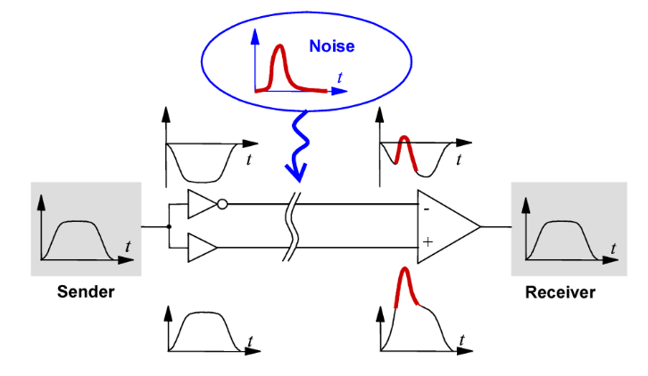
At its core, differential signaling involves transmitting information using two complementary signals (often called positive and negative, or P and N) that carry equal but opposite voltages. The receiving circuit detects the difference between these two signals rather than their absolute values relative to ground. When one line carries a positive voltage, the other carries an equal negative voltage, and vice versa.
For example, in a typical low-voltage differential signaling (LVDS) system:
- The positive signal might swing between +1.25V and +1.55V
- The negative signal would simultaneously swing between +1.55V and +1.25V
- The voltage difference represents the logical state (typically 300mV difference)
Comparison with Single-Ended Signaling
Traditional single-ended signaling uses one conductor referenced to ground, while differential signaling uses two conductors carrying opposite-phase signals. This fundamental difference leads to several key advantages:
- Noise Immunity: Common-mode noise (affecting both signals equally) is rejected because the receiver only cares about the difference between the signals.
- Reduced EMI: The opposing currents in the two conductors generate electromagnetic fields that tend to cancel each other out.
- Lower Voltage Swings: Differential signaling can operate with smaller voltage swings while maintaining good noise margins, enabling higher speeds with lower power consumption.
- Reference Independence: Unlike single-ended signals that require a clean reference plane, differential signals are self-referencing.
Key Characteristics of Differential Pairs
Impedance Considerations
Proper impedance control is critical for differential signaling. Designers must consider both the single-ended impedance of each trace and the differential impedance of the pair:
- Single-ended impedance (Z₀): The characteristic impedance of each individual trace to ground
- Differential impedance (Zdiff): The impedance between the two traces when driven differentially (typically 2×Z₀×(1-k), where k is the coupling coefficient)
- Common-mode impedance (Zcm): The impedance of both traces together to ground
Common differential impedance values include 100Ω (common in USB, Ethernet) and 90Ω (common in HDMI).
Coupling Types
Differential pairs can be implemented with different coupling approaches:
- Edge-coupled: Traces run side-by-side on the same layer
- Broadside-coupled: Traces are stacked vertically on adjacent layers
- Loose coupling: Increased spacing reduces interaction between traces
- Tight coupling: Minimal spacing maximizes interaction between traces
The choice depends on factors like layer stackup, routing density, and signal frequency requirements.
Length Matching
For differential signals to function properly, both traces in the pair must maintain precise length matching. Any length mismatch causes phase differences between the signals, leading to:
- Degraded signal quality
- Reduced common-mode rejection
- Potential timing violations
Typical length matching requirements range from 5 mils for moderate-speed interfaces to sub-mil tolerances for multi-gigabit designs.
PCB Design Considerations for Differential Pairs
Routing Best Practices
Proper routing of differential pairs requires attention to several key factors:
- Trace Geometry: Maintain consistent width and spacing throughout the entire route
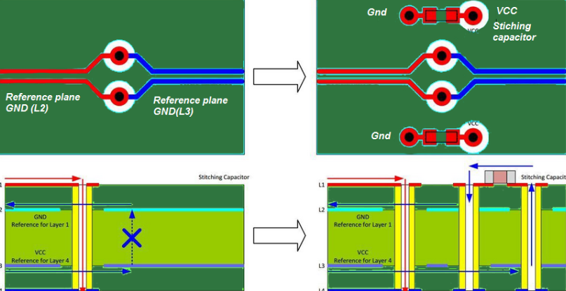
- Avoid Splits in Reference Planes: Keep a continuous return path beneath the pair
- Minimize Vias: Each via introduces impedance discontinuities
- Corner Handling: Use curved or 45° bends rather than 90° angles
- Separation from Other Signals: Maintain adequate clearance to prevent crosstalk
Termination Strategies
Proper termination is essential to prevent reflections that can degrade signal integrity:
- Resistive Termination: Matches the differential impedance at the receiver
- AC Coupling: Used when DC levels differ between transmitter and receiver
- Common-mode Termination: Sometimes added to suppress common-mode noise
Crosstalk Mitigation
While differential pairs offer inherent crosstalk resistance, designers must still consider:
- Spacing Between Pairs: Follow the 3W or 5H rules (3× trace width or 5× dielectric height)
- Layer Allocation: Route sensitive pairs on inner layers when possible
- Shielding: Use ground traces or vias as guards between critical pairs
Common Differential Signaling Standards
Several standardized interfaces use differential signaling, each with specific requirements:
- LVDS (Low-Voltage Differential Signaling): 100Ω differential impedance, common in displays and high-speed data links
- USB (Universal Serial Bus): 90Ω differential impedance for USB 2.0, more stringent requirements for USB 3.x
- PCI Express: 85Ω differential impedance with tight length matching requirements
- HDMI: 100Ω differential impedance for TMDS channels
- Ethernet (10/100/1000BASE-T): Various impedance requirements depending on standard
- DDR Memory Interfaces: Differential clocks and strobes with carefully controlled timing
Measurement and Verification
Verifying differential signal quality requires specialized techniques:
- Differential Probing: Use true differential probes to measure the actual signal difference
- Eye Diagram Analysis: Assess signal integrity by overlaying multiple unit intervals
- Time Domain Reflectometry (TDR): Measure impedance characteristics along the transmission line
- S-parameter Analysis: Evaluate frequency-domain performance in high-speed designs
Advanced Topics in Differential Signaling
Mixed-Mode S-Parameters
For comprehensive analysis of differential pairs, mixed-mode S-parameters separate measurements into:
- Differential mode (SDD): Desired signal transmission
- Common mode (SCC): Unwanted common-mode response
- Mode conversion (SCD, SDC): Conversion between differential and common modes
Equalization Techniques
At multi-gigabit speeds, various equalization methods compensate for channel loss:
- Transmit Pre-emphasis: Boosts high-frequency components
- Receiver Equalization: Compensates for inter-symbol interference
- Continuous-Time Linear Equalization (CTLE): Analog frequency response shaping
- Decision Feedback Equalization (DFE): Digital cancellation of post-cursor ISI
Return Loss Considerations
Maintaining good return loss (minimizing reflections) becomes increasingly important at higher frequencies:
- Impedance Control: Tight manufacturing tolerances on trace dimensions
- Via Optimization: Use back-drilling or micro-vias to minimize stubs
- Connector Selection: Choose connectors designed for high-speed differential signals
Practical Design Guidelines
To implement effective differential pairs in PCB designs:
- Stackup Planning: Allocate appropriate layers for differential routing early in design
- Design Rule Setup: Configure CAD tools with proper differential pair rules
- Simulation: Perform pre-layout and post-layout simulations
- Manufacturing Communication: Clearly specify requirements to PCB fabricators
- Test Planning: Design for testability with appropriate access points
Conclusion
Differential signaling has become indispensable in modern PCB design, enabling the high-speed data transmission required by today’s electronic systems. By understanding the principles of differential pairs and implementing proper design techniques, engineers can create robust, high-performance circuits capable of operating at multi-gigabit data rates while maintaining signal integrity and minimizing EMI.
As data rates continue to increase with each new generation of electronic devices, the importance of proper differential pair design only grows. Future developments in materials, manufacturing processes, and design methodologies will continue to push the boundaries of what’s possible with differential signaling, but the fundamental principles covered in this article will remain relevant for years to come.
Mastering differential signal design requires both theoretical knowledge and practical experience, but the effort pays dividends in the form of reliable, high-performance electronic systems. By applying the concepts and techniques discussed here, PCB designers can effectively implement differential signaling in their projects and overcome the challenges of high-speed digital design.