What Are PCB Test Points?
Introduction to PCB Test Points
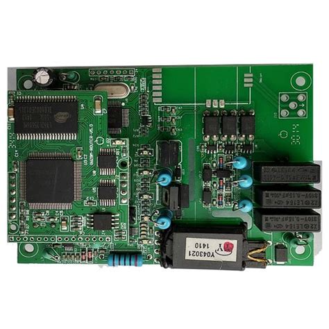
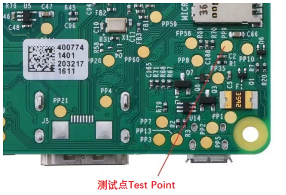
Printed Circuit Board (PCB) test points are specific locations on a circuit board designed to facilitate testing during manufacturing, debugging, and maintenance processes. These dedicated contact points allow engineers and technicians to measure electrical signals, verify circuit functionality, and diagnose potential issues without damaging the board or its components.
Test points serve as the primary interface between the PCB and testing equipment, enabling various types of electrical measurements throughout the product lifecycle—from initial prototype verification to final quality assurance checks in mass production. Properly implemented test points significantly improve testing efficiency, reduce inspection time, and enhance the overall reliability of electronic devices.
The Purpose of Test Points in PCB Design
Test points fulfill several critical functions in PCB development and manufacturing:
- Manufacturing Testing: During production, test points allow automated test equipment (ATE) to verify that components are correctly placed and soldered, and that the board functions as intended.
- Debugging and Troubleshooting: Engineers use test points to isolate problems during development or when analyzing field returns.
- Quality Control: Test points enable sampling inspection of production boards to ensure consistent quality.
- Functional Verification: They provide access to key signals for validating that the circuit performs its intended function.
- Programming and Configuration: Some test points serve as interfaces for programming firmware or configuring devices.
Without properly designed test points, testing becomes more difficult, time-consuming, and potentially damaging to the PCB, as technicians might need to probe component pins directly or use makeshift contact methods.
Types of PCB Test Points
PCB test points come in various forms, each suited to different testing requirements and stages of the product lifecycle:
1. Bare Board Test Points
Used for testing the PCB before component population, these points verify:
- Continuity (no open circuits)
- Isolation (no short circuits)
- Impedance characteristics (for high-speed designs)
2. In-Circuit Test (ICT) Points
Designed for automated testing after component assembly, ICT points:
- Are typically larger (50-100 mil diameter)
- Have sufficient spacing for bed-of-nails test fixtures
- Provide access to all critical nodes in the circuit
3. Functional Test Points
Used for system-level verification, these points:
- May be smaller than ICT points
- Often focus on key functional signals
- Sometimes include labeled headers or connectors
4. Debug Test Points
Designed for engineering use, these points:
- Provide access to important internal signals
- May include ground reference points nearby
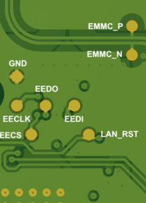
- Are often labeled with signal names or test conditions
5. Boundary Scan Test Points
For JTAG-compliant devices, these points:
- Form part of the boundary scan chain
- Enable testing of complex digital circuits
- Require specific pin assignments (TDI, TDO, TCK, TMS)
Physical Characteristics of Test Points
Effective test points share several physical characteristics:
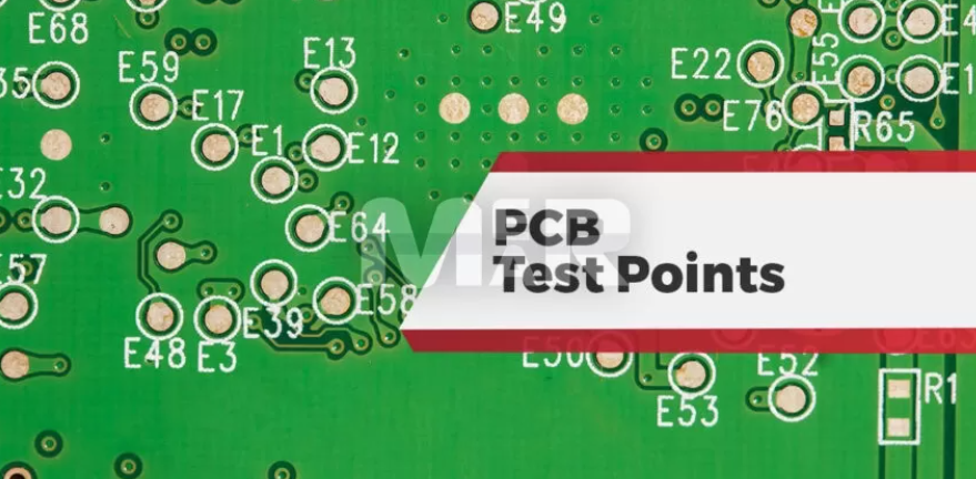
- Size and Shape: Typically round pads (30-100 mil diameter) or square pads for better probe contact. Larger sizes accommodate automated probing.
- Spacing: Adequate clearance between test points (typically ≥100 mil center-to-center) prevents probe shorting.
- Surface Finish: Often use robust finishes like gold plating (hard or soft) over nickel to withstand repeated probing.
- Location: Preferably placed on the solder side of the board, away from tall components, with consistent spacing for test fixture alignment.
- Annular Ring: Sufficient copper around the via (if used) ensures reliable contact after multiple probe touches.
- Labeling: Silkscreen labels identifying test point function improve usability, though space constraints may limit this in dense designs.
Design Considerations for PCB Test Points
Implementing effective test points requires careful planning during the PCB design phase:
1. Test Coverage Strategy
Determine which signals need testing based on:
- Critical circuit functions
- Fault detection requirements
- Manufacturing defect probabilities
- Accessibility of signals through other means (like boundary scan)
2. Physical Layout Guidelines
- Place test points on a grid (typically 100 mil) for automated test fixtures
- Maintain consistent orientation (all test points facing the same direction)
- Keep test points ≥50 mil from component edges
- Avoid placing under components or in hard-to-reach areas
3. Electrical Considerations
- Include ground test points near signal test points for reference
- For high-frequency signals, consider impedance-matched test points
- Ensure test points don’t load sensitive circuits excessively
4. Manufacturing Requirements
- Consult with your PCB manufacturer about minimum test point sizes
- Coordinate with test engineering on fixture requirements
- Consider panelization effects if testing boards before separation
5. Documentation
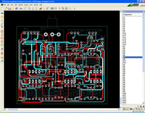
- Include test points in schematics (often as special symbols)
- Maintain a test point list in design documentation
- Provide coordinate files for automated test programming
Test Point Implementation Techniques
Several methods exist for implementing test points in PCB designs:
1. Dedicated Test Pads
Simple copper pads not connected to components, used solely for testing. Advantages:
- No effect on circuit operation
- Can be placed optimally for probing
Disadvantages: - Consume additional board space
2. Component Pads as Test Points
Using existing component pads (like resistor ends) as test points. Advantages:
- Saves space
- Reduces design effort
Disadvantages: - May be inaccessible after assembly
- Probing may damage components
3. Via Test Points
Using plated through-hole vias as test points. Advantages:
- Saves space (can be placed under components)
- Provides access to inner layers
Disadvantages: - Smaller contact area
- More challenging for repeated probing
4. Castellated Test Points
Half-cut holes along board edges that serve as both test points and mounting features. Common in module designs.
5. Header Connectors
Multi-pin headers that provide grouped test access. Useful for functional testing but less so for manufacturing tests.

Testing Methodologies Using Test Points
Different testing phases utilize test points in various ways:
1. Bare Board Testing
Verifies PCB fabrication quality by checking:
- Continuity between connected test points
- Isolation between unrelated test points
- Impedance on controlled lines
2. In-Circuit Testing (ICT)
Uses a bed-of-nails fixture to contact all test points simultaneously for:
- Component presence and orientation checks
- Short/open circuit detection
- Basic functional verification
3. Flying Probe Testing
Moving probes contact test points sequentially, suitable for:
- Low-volume production
- Prototype testing
- Boards with limited test point access
4. Functional Testing
Verifies overall system operation through selected test points, typically:
- Power supply measurements
- Key signal validation
- Interface testing
5. Boundary Scan Testing
Uses JTAG test points to verify digital circuits through their I/O boundaries, especially useful for:
- High-density boards
- BGA components
- Complex digital systems
Advanced Test Point Considerations
Modern PCB designs present unique test point challenges:
1. High-Density Designs
With component spacing shrinking, test point implementation requires:
- Micro-test points (smaller than traditional sizes)
- Alternative access methods (like via probing)
- Careful planning to maintain test coverage
2. High-Speed Signals
Testing high-frequency signals demands:
- Impedance-matched test points
- Minimal stub lengths
- Careful consideration of probe loading effects
3. RF and Microwave Circuits
Require specialized test point approaches:
- Controlled impedance test ports
- Minimal disruption to transmission lines
- Often use coaxial connectors instead of standard test points
4. Mixed-Signal Systems
Need separate consideration for:
- Analog test points (noise sensitivity)
- Digital test points (timing considerations)
- Power supply test points (current requirements)

Best Practices for Test Point Design
To maximize testing effectiveness while minimizing board impact:
- Early Planning: Incorporate test point strategy from the initial design phase.
- Balance Coverage and Practicality: Include test points for critical signals but avoid excessive coverage that complicates layout.
- Standardize Approaches: Use consistent test point styles throughout the design for easier fixture development.
- Consider All Testing Phases: Ensure test points support prototyping, production, and field service needs.
- Collaborate with Stakeholders: Involve manufacturing and test engineers in test point planning.
- Document Thoroughly: Clearly identify all test points in design documentation.
- Validate Before Finalizing: Verify test point accessibility with physical mockups if necessary.
Common Test Point Design Mistakes
Several frequent errors can compromise test effectiveness:
- Insufficient Test Coverage: Missing critical signals that need verification.
- Poor Physical Placement: Test points blocked by components or too close for reliable probing.
- Inadequate Size or Spacing: Making contact difficult for test probes.
- Missing Ground References: No nearby ground points for signal measurements.
- Overlooking Fixture Requirements: Not accounting for mechanical constraints of test equipment.
- Ignoring Signal Integrity: Test points that degrade circuit performance.
- Inconsistent Implementation: Varying test point styles that complicate testing procedures.
Future Trends in PCB Test Point Technology
Emerging developments are shaping test point evolution:
- Embedded Probing: Technologies allowing contactless or minimally invasive signal access.
- Design-for-Test Automation: Tools that automatically optimize test point placement.
- Advanced Fixture Technologies: Higher density probing solutions for complex boards.
- Integrated Self-Test: More circuits incorporating built-in test capabilities reducing external test point needs.
- 3D-PCB Considerations: Test strategies for multilayer and embedded component designs.
Conclusion
PCB test points represent a critical bridge between design intent and real-world functionality. By providing controlled access to circuit signals, they enable efficient verification of manufacturing quality, design performance, and long-term reliability. Effective test point design requires balancing multiple considerations—from physical constraints to electrical requirements—while anticipating all stages of the product lifecycle.
As electronic systems grow more complex, the importance of thoughtful test point implementation only increases. Engineers who master test point design principles contribute significantly to product quality, manufacturing efficiency, and serviceability. While test points may seem like simple features, their proper implementation often distinguishes between a design that’s merely functional and one that’s truly robust and manufacturable.
In an era of ever-shrinking components and rising quality expectations, test points remain an essential tool for ensuring PCB reliability. Their continued evolution will parallel advancements in electronics manufacturing, maintaining their vital role in bringing reliable products to market.