What are the things to pay attention to in PCB layout?
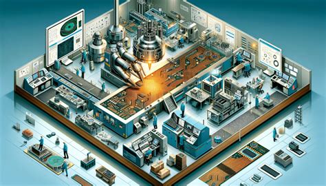
Printed circuit board (PCB) layout may be considered an art form by circuit designers, and there is a lot of truth to that. Creating the most reliable, functional, and cost-effective circuits and finished PCBs can be a challenging task, especially with today’s demand for increasingly complex requirements for compact, lightweight, and even flexible circuit boards.
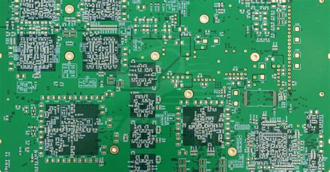
The first considerations in PCB layout are size and shape. The end result must fit the environment in which the board will be installed and used, driving the design process. Space considerations may require the use of multilayer or high-density interconnect (HDI) designs. Some projects require specialized board shapes and weight restrictions, making layout particularly challenging.
While this may not be a major consideration when designing initial circuit functions, in situations such as prototyping, it becomes a higher priority when laying out PCBs for production manufacturing.
Consider your manufacturer during the PCB layout stage. Not all manufacturers can produce higher-volume multilayer boards or HDI PCBs. Most cases require PCB layout designs that incorporate technologies such as flexible or flex-rigid construction, which require review with the proposed supplier to ensure that the layout design and material requirements are met.
Special requirements, such as the need to employ lead-free construction or otherwise avoid potentially hazardous materials, can be a critical point in making layout and construction decisions.
Technical PCB Layout Issues
Other more technical factors to consider in PCB layout:
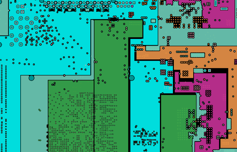
Trace widths
Spacing between traces
Tolerances for electrical factors that may affect the functionality of the board
Clearing traces and components from trace edges
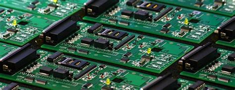
Component availability – Hard-to-find or specialized components can significantly increase the cost of the final board. This can be a major issue if lower-cost alternatives can be produced and large volumes of boards are expected to be produced.
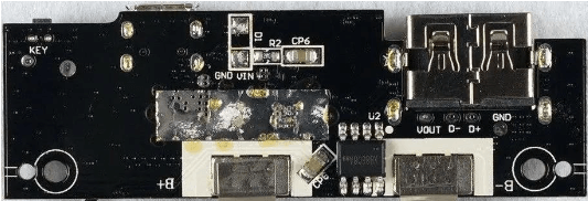
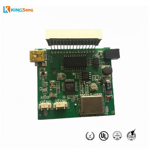
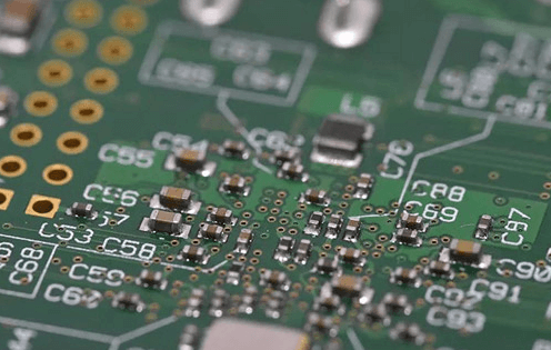
Construction Methods – PCB layout is largely determined by the physical construction of the board: through-hole assembly, surface mount technology (SMT), or a combination of the two. Multilayer and HDI board design has evolved rapidly in recent years, with many specific layout requirements for these technologies.
Importance of PCB Layout
Lack of efficient and accurate layout can lead to a nearly endless number of problems, including:
Electromagnetic interference from conflicting component or trace placement
Conflicts of components on both sides of the board
Rework and manufacturing delays for designers
Limited board functionality
Total board failure
Solving Many PCB Layout Problems
Most PCB designers and manufacturers today have access to sophisticated computer-aided design (CAD) and computer-aided manufacturing (CAM) software systems. These professional programs have many advantages over traditional engineering methods:
Drag-and-drop design – Easily and accurately place components, then let the software generate the traces to connect. Move or add components easily and quickly.
Layout Verification – Tolerances, compatibility, component placement, etc. are verified during design and before releasing the PCB for manufacturing, or even prototyping.
Reuse – Once a layout is approved and saved, it can be reused as a template for new PCB projects and used by other engineers.
Efficiency – Using these professional programs can speed up development, reduce errors, and improve time to market.
Cost Savings – Efficiency equates to savings from redesign or manufacturing errors.
Error Detection – Catch basic errors in real time, avoiding defects in manufacturing or delays in detection by the manufacturer.
Rule Creation – Many of these programs support the creation of custom rule sets specific to the designer’s purpose. Creating these rules and storing them allows designers to share and enhance the functionality of the software.
Documentation – Designs can generate detailed documentation on component use, error reporting, design status, revisions
Generate Manufacturing Files – Quickly and easily create Gerber files or other formats for manufacturers, ensuring accurate manufacturing specifications, including component placement, specifications, traces, silkscreens, solder masks, and drill files.
Always keep Design for Manufacturing (DFM) in mind during PCB layout and design. The most brilliant and creative PCB layout is of little value if it cannot be manufactured within the project budget, or if the designated manufacturer cannot manufacture it.