What are the wiring principles of PCB boards? And what are the skills in wiring?
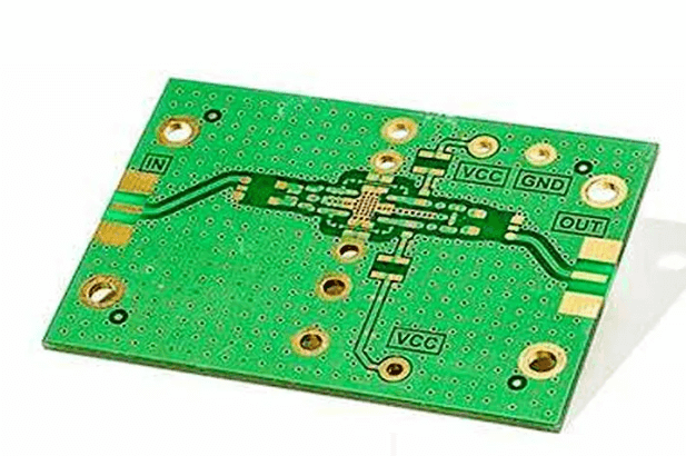
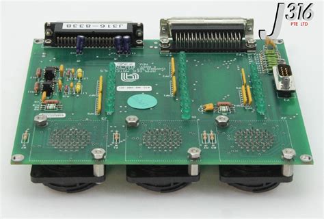
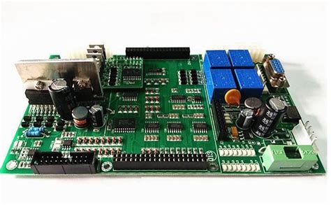
Printed circuit boards (PCBs) are an indispensable part of electronic equipment, and their performance and reliability directly affect the operation of the entire system. PCB (Printed Circuit Board), Chinese name for printed circuit board, also known as printed circuit board, is an important electronic component, a support for electronic components, and a carrier for electrical interconnection of electronic components. Because it is made using electronic printing, it is called a “printed” circuit board.
Wiring is a key step in PCB design, which determines the performance and stability of the circuit board. This article will explore the wiring principles of PCB boards and some practical tips to help engineers get better results in design.
2.Wiring principles
Follow the circuit schematic
Wiring should strictly follow the circuit schematic to ensure that the line is connected correctly to prevent short circuits or open circuits. During the wiring process, each component in the circuit should be marked for subsequent maintenance and repair.
Consider the signal direction
When wiring, it is necessary to consider the direction of the signal and make the signal line as short as possible to reduce signal attenuation and noise. For high-frequency signals, attention should be paid to the impedance matching of the signal line to avoid signal reflection and distortion.
Layered wiring
In a multi-layer PCB, the wiring should be layered according to the function of the circuit. For example, the power layer and the ground layer can be routed separately to reduce the noise of the power supply and the ground. Different signal layers can also be routed in layers to avoid interference between signals.
Avoid 90-degree bends
During the transmission process, the signal line should avoid 90-degree bends as much as possible. Because this bend will increase the reflection and noise of the signal and affect the quality of the signal. If a 90-degree bend must be made, a 45-degree bend or an arc bend should be used for transition.
Ground wire design
The design of the ground wire is crucial to the reliability of the PCB. During the wiring process, the ground wire should be as wide as possible to reduce the impedance of the ground wire and improve the stability of the ground wire. At the same time, the 90-degree bend of the ground wire should be avoided to ensure the continuity of the ground wire.
3.Wiring skills
Use automatic wiring tools
Modern circuit design software usually provides automatic wiring functions, which can greatly simplify the wiring process. Automatic wiring tools can automatically allocate lines according to the circuit schematic, optimize wiring paths, and reduce conflicts. When using the automatic routing tool, some manual adjustments can be made as needed to achieve better routing results.
Post-routing inspection
After the routing is completed, a series of inspections should be carried out to ensure the correctness and reliability of the routing. For example, the continuity, conductivity and impedance matching of the signal line, as well as the stability of the power supply and ground line can be checked. In addition, the circuit can be simulated using simulation tools to verify the performance and reliability of the circuit.
Reasonable use of filling and copper cladding
During the routing process, filling and copper cladding can be used to improve the performance and stability of the PCB. Filling can be used to fill the gaps on the circuit board to improve the mechanical strength and thermal stability of the circuit board. Copper cladding can be used as a ground line or power line to increase the reliability and stability of the circuit. However, it should be noted that filling and copper cladding may also cause uneven thermal expansion coefficients of the circuit board, which needs to be weighed in the specific design.
Routing optimization
During the routing process, some optimizations can be made to improve the performance and stability of the circuit. For example, the width and spacing of the signal line, the layout of the ground line, the direction of the power line, etc. can be optimized to reduce problems such as signal reflection, noise and crosstalk. In addition, you can also consider using differential pair wiring technology to improve signal integrity and reliability.
Accumulation of experience and skills
Wiring is a job that requires experience and skills, and requires continuous accumulation of experience in practice. Engineers should pay attention to the latest wiring technology and tools, learn from the experience and methods of other designers, and continuously improve their wiring skills and design capabilities. At the same time, simulation tools can also be used for virtual testing to verify the feasibility and reliability of the design before actual production.
IV. Summary
In short, PCB board wiring is a job that requires following basic principles and using skills. Engineers need to reasonably plan wiring paths and optimize wiring skills based on understanding the circuit schematic to improve the performance and stability of the circuit. At the same time, it is also necessary to pay attention to the accumulation of experience and the use of tools to obtain better results in the design process.