What is PCB heat dissipation hole? How to set PCB heat dissipation hole?
When designing PCB, in many cases we need to dissipate heat for certain components (such as linear regulators). In most cases, these settings are universal through-hole components, because the heat sink can effectively dissipate heat in the aluminum area and use the device to keep in cooler ambient conditions. But if we talk about any SMD device, the heat sink is not available, and most of the time. It is necessary to use copper cladding technology to create a sufficient heat sink on the copper layer.
1.What is PCB heat dissipation hole?
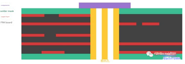
Heat dissipation hole is a method of using channels (vias) that penetrate the PCB board to conduct heat to the back to dissipate heat. It is configured directly below the heating element or as close to the heating element as possible. Heat dissipation hole is a method of using PCB board to improve the heat dissipation effect of surface mount components. In terms of structure, through holes are set on the PCB board.
If it is a single-layer double-sided PCB board, the copper foil on the surface and back of the PCB board is connected to increase the area and volume for heat dissipation, that is, to reduce thermal resistance.
If it is a multi-layer PCB board, the surfaces between the layers can be connected or the layers with limited connection can be limited, etc. The purpose is the same.
2.How to set up PCB heat dissipation holes?
The placement and size of PCB heat dissipation holes vary greatly, depending on the type of component, different rules and expertise.
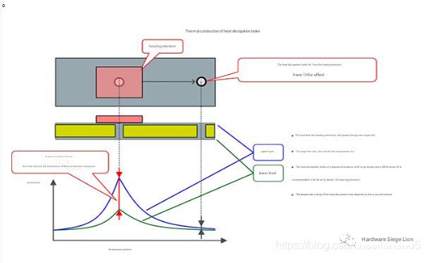
But a main rule is to use heat dissipation holes as close to the heat source directly below the heating element as possible. Then in the case of an undesirable heat source, thermal vias can also be placed on the periphery of the component regardless of the component pad placement. In this case, the rule also remains the same, that is, to place the heat dissipation holes as close to the periphery of the group as possible. To use heat dissipation holes effectively, it is important to configure the heat dissipation holes close to the heating body, such as directly below the component. As shown in the figure below, it can be seen that it is a good method to use the heat balance effect to connect the position with a large temperature difference.
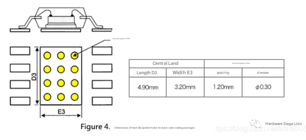
PCB heat dissipation hole placement example Example: Configuration of heat dissipation holes The following is an example of the layout and size of the heat dissipation holes for the HTSOP-J8 package with exposed heat sink on the back.
3.How big are the heat dissipation holes in general on PCB?
To improve the thermal conductivity of the heat dissipation holes, it is recommended to use small-diameter through holes with an inner diameter of about 0.3mm that can be filled with electroplating. It should be noted that if the hole diameter is too large, solder creeping may occur during the reflow process. The heat dissipation holes are spaced about 1.2mm apart and are configured directly below the heat sink on the back of the package. If the heat dissipation directly below the heat sink on the back is not enough, heat dissipation holes can also be configured around the IC. The key point of the configuration in this case is to configure it as close to the IC as possible.
Heat via size
4. Thermal conductivity of different materials
Thermal conductivity is a key factor that determines how much heat a material can absorb. The following table can understand the thermal conductivity of different materials. With the help of this table, you can have a certain reference See the table below:
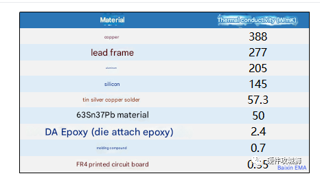
So, from the above table, it can be seen that aluminum has a worse thermal conductivity than copper. However, since the aluminum heat sink has a larger area, it produces a more effective cooling effect on the heated device. However, as we can see, if copper is used effectively, it can dissipate more heat than the same area of aluminum. Effective thermal via placement is when the via is used appropriately in the IC or heating element pad using conduction, as a heat transfer method, the heat is distributed between multiple layers of copper, and then through free air, the heat dissipation begins to be transferred in the air using convection methods. It is recommended that the inner diameter of the thermal via needs to be smaller, such as about 0.35 mm. If the aperture is larger, there may be problems with incorrect soldering during the reflow process, so extra care is needed. However, if a larger diameter is required, thermal filling may help compensate for this.
5.PCB Thermal Via Design Considerations
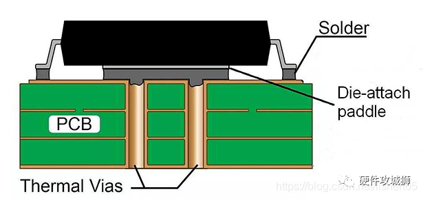
There are few things to note during the thermal via design process, and the following 6 suggestions are given. 1. The exposed pad is designed in a way that heat is transferred directly from the shell to the copper area. The effect of solder as a heat sink is not obvious because it is thin and the conductivity of solder is poor.

The above figure shows the thermal via on the exposed pad of U1.
- For the exposed pad package, the greatest heat dissipation occurs through the via to the bottom layer of the PCB and then dissipates into the air. Therefore, a large area of the bottom layer will also reduce the heat dissipation of the component package.
- Separating the heated components and using thermal vias for heat dissipation helps to evenly distribute the heat to other packages.
- Thermal vias are the only source of heat dissipation on DFN and QFN packages because the top copper does not have maximum space due to the pinout. Therefore, to use the bottom copper, the only way to increase thermal conductivity is to use thermal vias.
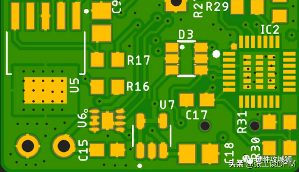
U5 and IC2 use thermal vias. IC2 uses a QFN flat package, where thermal vias are the only possible because this does not include a larger copper area on the solder layer due to the distribution of component pads. 5. The effective copper area of the thermal via connected device will be the maximum copper length that can be directly connected to the component package using thermal vias (regardless of the solder layer). 6. The thickness of the copper plane also affects thermal conductivity, and 2Oz copper has better heat resistance than 1.0 Oz or 0.5Oz copper. These are some suggestions for using heat dissipation holes, I hope they can help engineers who need to consider heat dissipation equipment in their designs. The above is some knowledge about PCB heat dissipation holes. I hope you can support me and leave a message in the comment area for discussion.