What is PCB.What are the precautions in PCB processing?
PCB has many functions in electronic equipment, such as providing certain electrical functions. In order to enhance everyone’s understanding of PCB, this article will introduce the basic situation of PCB and the precautions for successful PCB processing. If you are interested in PCB or the content of this article, you may wish to continue reading with the editor.
1.PCB
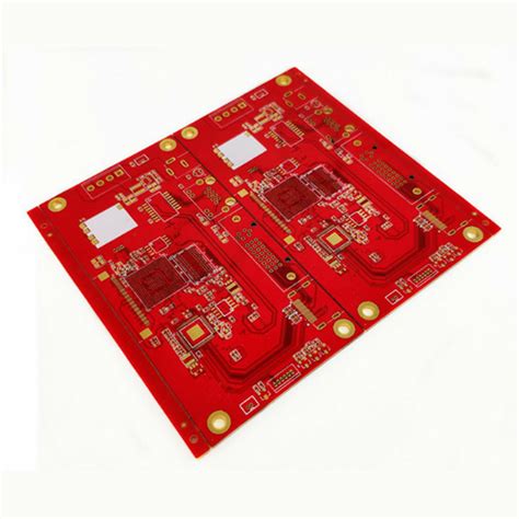
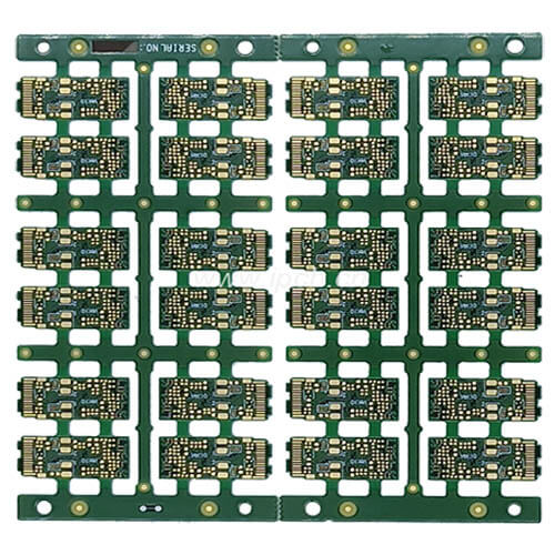
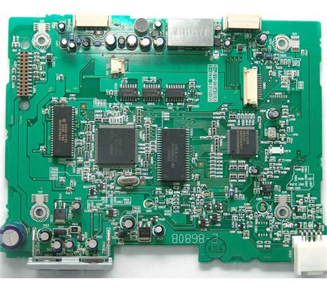
PCB (printed circuit board) is a printed circuit board, abbreviated as printed board, which is one of the important components of the electronics industry. Almost every electronic device, from electronic watches and calculators to computers, communication electronic equipment, and military weapon systems, as long as there are electronic components such as integrated circuits, in order to make the electrical interconnection between the components, a printed circuit board must be used.
The printed circuit board consists of an insulating base plate, connecting wires, and pads for assembling and welding electronic components. It has the dual functions of a conductive circuit and an insulating base plate. It can replace complex wiring to realize the electrical connection between the components in the circuit, which not only simplifies the assembly and welding of electronic products, reduces the wiring workload under the traditional method, and greatly reduces the labor intensity of workers; but also reduces the size of the whole machine, reduces product costs, and improves the quality and reliability of electronic equipment.
Printed circuit boards have good product consistency.
They can adopt standardized designs, which is conducive to mechanization and automation in the production process. At the same time, the entire assembled and debugged printed circuit board can be used as an independent spare part, which is convenient for the interchange and maintenance of the whole machine product. At present, printed circuit boards have been widely used in the production and manufacturing of electronic products.
The earliest printed circuit boards used were paper-based copper-clad printed circuit boards.
Since the emergence of semiconductor transistors in the 1950s, the demand for printed circuit boards has risen sharply. In particular, the rapid development and widespread application of integrated circuits have made the size of electronic equipment smaller and smaller, and the density and difficulty of circuit wiring have become increasingly greater, which requires printed circuit boards to be constantly updated. At present, the varieties of printed circuit boards have developed from single-sided boards to double-sided boards, multi-layer boards and flexible boards; the structure and quality have also developed to ultra-high density, miniaturization and high reliability; new design methods, design supplies and board materials, board making processes continue to emerge. In recent years, various computer-aided design (CAD) printed circuit board application software has been popularized and promoted in the industry. In specialized printed circuit board manufacturers, mechanized and automated production has completely replaced manual operations.
2.Precautions during PCB processing
1) PCB before cutting
The purpose of baking the PCB before cutting the copper-clad board (150℃, time 8±2 hours) is to remove moisture from the board, and at the same time completely solidify the resin in the board, and further eliminate the residual stress in the circuit board, which is very useful for preventing the circuit board from warping.
At present, many double-sided and multi-layer boards still insist on the baking steps before or after unloading. However, some board factories have exceptions. At present, the drying time of PCB factories is also inconsistent, ranging from 4 to 10 hours. It is recommended to decide according to the grade of the printed board produced and the customer’s requirements for warping.
After the whole piece is baked, it is cut into puzzles or baked after unloading. Both methods are feasible. It is recommended to bake the board after cutting, and the inner board should also be baked.
2) Latitude and longitude of prepreg
After the prepreg is bonded, the shrinkage rate in the latitude and longitude is different. The latitude and longitude must be distinguished during blanking and bonding, otherwise it is easy to cause the finished board to warp after bonding, and it is difficult to correct even if pressure is applied to the baking board.
Many of the reasons for the warping of multilayer boards are due to the fact that the prepregs are not distinguished in the warp and weft directions during lamination and are randomly stacked.
How to distinguish the warp and weft? The rolling direction of rolled prepregs is the warp direction and the width direction is the weft direction; for copper foil boards, the long side is the weft direction and the short side is the warp direction. If you are not sure, you can ask the manufacturer or supplier.
3) Stress relief after lamination
After hot pressing and cold pressing, the multilayer board is taken out, cut or milled to remove the burrs, and then placed flat in an oven at 150℃ for 4 hours to gradually release the stress in the board and completely cure the resin. This step cannot be omitted.
4) Thin boards need to be straightened during electroplating
When 0.4-0.6mm ultra-thin multilayer boards are used for surface electroplating and pattern electroplating, special clamping rollers should be made. After clamping the thin board on the clamping roller on the automatic electroplating line, clamp the entire clamping roller with a round bar. String the rollers together and straighten all the sheets on the rollers so that the electroplated sheets will not deform.
Without this measure, after electroplating a 20 to 30um copper layer, the board will bend and it is difficult to remedy.
5) Cooling of the board after hot air leveling
When the PCB is leveled with hot air, it will be affected by the high temperature of the solder bath (about 250℃). After taking it out, it should be placed on a flat marble or steel plate to cool naturally, and then sent to the post-processing machine for cleaning, which is conducive to preventing the circuit board from warping.
In order to improve the brightness of the lead-tin surface, some factories put the board into cold water immediately after hot air leveling, and take it out for post-processing after a few seconds. This hot and cold shock may cause some types of circuit boards to warp. Distortion, delamination or blistering.