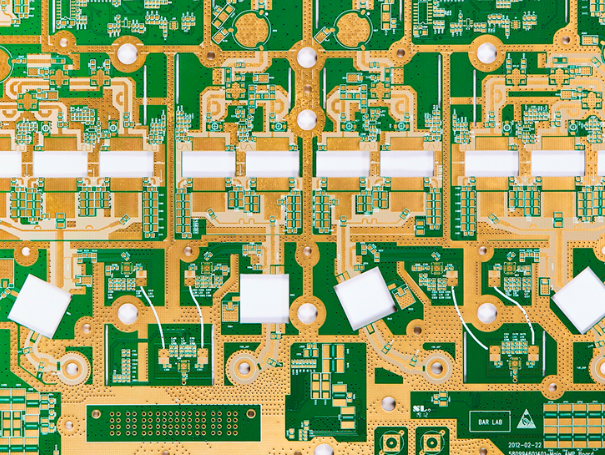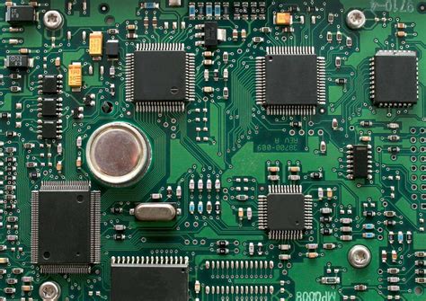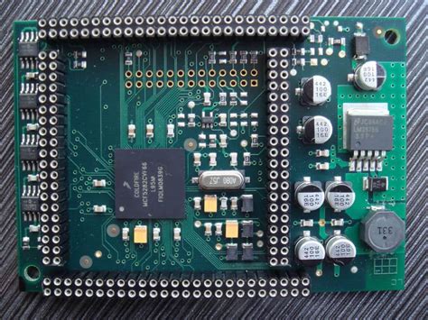
When designing PCB, please don’t fall into these 10 pitfalls
1.Unclear definition of processing level
Single-sided board design is on the TOP layer. If it is not explained whether to do it on the front and back, the board may not be easy to solder when the device is installed.
2.Large area copper foil is too close to the outer frame
The large area copper foil should be at least 0.2mm away from the outer frame, because when milling the shape, if the copper foil is milled, it is easy to cause the copper foil to warp and the solder resist to fall off.
3.Use filler blocks to draw pads
Using filler blocks to draw pads can pass DRC inspection when designing circuits, but it is not possible for processing, because such pads cannot directly generate solder resist data. When applying solder resist, the filler block area will be covered by solder resist, making it difficult to solder the device.
4.The electrical ground layer is both a flower pad and a connection line
Because the power supply is designed as a flower pad, the ground layer is opposite to the image on the actual printed circuit board, and all the connections are isolated lines. Be careful when drawing several groups of power supplies or several ground isolation lines. Do not leave gaps to short-circuit the two groups of power supplies, nor block the connection area.
5.Random placement of characters
The characters cover the pad SMD solder piece, which brings inconvenience to the continuity test and component welding of the printed circuit board. If the character design is too small, it will cause screen printing difficulties. If it is too large, the characters will overlap and be difficult to distinguish.
6.The surface mount device pad is too short
This is for the continuity test. For too dense surface mount devices, the distance between the two feet is quite small, and the pad is also quite thin. When installing the test needle, it must be staggered up and down. If the pad design is too short, although it does not affect the device installation, it will make the test needle misaligned.
7.Single-sided pad aperture setting
Single-sided pads are generally not drilled. If the drilling needs to be marked, the aperture should be designed to be zero. If the numerical value is designed, the hole coordinates will appear at this position when the drilling data is generated, and problems will occur. Single-sided pads should be specially marked if drilling is performed.
8.pad overlap
Drilling multiple times in one place will cause the drill bit to break, resulting in hole damage. Two holes overlap in a multilayer board, and after drawing the negative, it appears as an isolation disk, causing scrap.
9.There are too many filling blocks in the design or the filling blocks are filled with very fine lines
The generated photolithography data is lost, and the photolithography data is incomplete. Because the filling blocks are drawn one by one with lines when processing photolithography data, the amount of photolithography data generated is quite large, which increases the difficulty of data processing.
10.Abuse of graphic layers
Some useless connections are made on some graphic layers. The original four-layer board is designed with more than five layers of lines, which causes misunderstandings. It violates conventional design. The graphic layer should be kept complete and clear during design.