Why Are Most PCBs 1.6mm Thick? The History and Practical Reasons Behind the Standard PCB Thickness
Introduction
Printed Circuit Boards (PCBs) form the foundation of nearly all modern electronics, from smartphones to industrial control systems. Among the various specifications that define a PCB, thickness stands out as one of the most fundamental—and one where 1.6mm (approximately 0.063 inches) has emerged as the de facto standard for countless applications. This article explores the historical origins, technical rationale, manufacturing considerations, and modern alternatives surrounding this ubiquitous dimension that has shaped electronics manufacturing for decades.
The Historical Origins of 1.6mm PCB Thickness
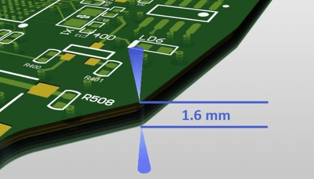
The story of 1.6mm PCB thickness begins in the early days of the electronics industry in the United States during the mid-20th century. As PCB technology transitioned from laboratory curiosity to mass production, manufacturers needed to standardize dimensions to ensure compatibility across components and systems.
In the imperial measurement system dominant in U.S. manufacturing at the time, 1/16 of an inch became a convenient reference point for PCB thickness. This measurement equates to:
- 1/16 inch = 0.0625 inches
- 0.0625 inches ≈ 1.5875mm (rounded to 1.6mm in metric)
This thickness emerged as a practical compromise between several competing factors:
- Mechanical stability: Thinner boards risked warping or breaking during handling
- Component compatibility: Accommodated through-hole components with standard lead lengths
- Manufacturing limitations: Early PCB fabrication techniques worked best within this range
- Cost considerations: Balanced material costs with performance requirements
The 1/16-inch standard became deeply embedded in component designs, fabrication equipment, and industry specifications. Even as the global electronics industry transitioned to metric measurements, the 1.6mm metric equivalent maintained dominance due to existing infrastructure and tooling.
Technical Advantages of 1.6mm Thickness
Mechanical Stability and Rigidity
The 1.6mm thickness provides optimal mechanical properties for most applications:
- Sufficient rigidity to prevent excessive flexing during handling or operation
- Resistance to warping during soldering processes (especially wave soldering)
- Ability to support medium-weight components without additional reinforcement
- Compatibility with standard edge connectors and board guides
Electrical Performance Characteristics
From an electrical perspective, 1.6mm boards offer:
- Adequate spacing between layers for controlled impedance in typical digital circuits
- Reduced crosstalk compared to thinner boards in multilayer configurations
- Manageable parasitic capacitance for many analog and digital applications
- Suitable dielectric thickness for common voltage requirements
Thermal Management Properties
The thickness affects heat dissipation:
- Provides enough thermal mass for moderate heat loads
- Allows effective heat transfer to mounting surfaces or heatsinks
- Balances thermal expansion characteristics with common component materials
Manufacturing and Assembly Considerations
Fabrication Process Compatibility
1.6mm thickness aligns well with PCB manufacturing processes:
- Works with standard laminate stock sizes
- Compatible with drilling and routing equipment
- Optimal for plating processes (hole wall thickness requirements)
- Fits within typical layer count to thickness ratios
Assembly Process Optimization
The thickness supports efficient assembly:
- Withstands wave soldering temperatures without warping
- Accommodates standard component lead lengths
- Provides sufficient z-axis expansion for plated through holes
- Works with automated handling equipment
Cost Efficiency Factors
1.6mm represents a cost-effective balance:
- Material usage versus performance
- Panel utilization in fabrication
- Yield rates in production
- Compatibility with standard components and enclosures
The Evolution of PCB Thickness Standards
While 1.6mm remains dominant, the PCB industry has developed a range of standard thicknesses to accommodate different needs:
Common Standard Thicknesses
- 0.4mm (ultra-thin for compact devices)
- 0.8mm (common in consumer electronics)
- 1.0mm (increasingly popular for space-constrained designs)
- 1.2mm (alternative mid-range option)
- 1.6mm (standard thickness)
- 2.0mm+ (for high-power or rigid applications)
Factors Driving Thinner Boards
Modern electronics trends have increased demand for thinner PCBs:
- Miniaturization of consumer devices
- Flexible and rigid-flex PCB adoption
- High-density interconnect (HDI) technologies
- Portable and wearable electronics requirements
Niche Applications for Thicker Boards
Some applications still require greater thickness:
- High-power electronics needing improved heat dissipation
- Boards with extreme mechanical load requirements
- Specialized RF and microwave applications
- Certain automotive or aerospace applications
Modern Alternatives and the Future of PCB Thickness
While 1.6mm remains the baseline, several factors are changing thickness considerations:
High-Density Interconnect (HDI) Technologies
HDI designs often use thinner substrates to enable:
- Microvias and advanced via structures
- Finer trace widths and spacing
- Increased layer count in same form factor
Flexible and Rigid-Flex PCBs
These technologies employ thin, flexible materials:
- Typical thicknesses from 0.1mm to 0.3mm
- Enables folding and bending in final products
- Requires different design approaches
Advanced Materials and Manufacturing
New materials and processes affect thickness choices:
- High-frequency laminates with different dielectric properties
- Embedded component technologies
- Additive manufacturing approaches
Conclusion: Why 1.6mm Endures
Despite evolving technologies and applications, 1.6mm PCB thickness maintains its dominant position due to:
- Historical Momentum: Decades of infrastructure, tooling, and component design based on this standard
- Technical Balance: Optimal compromise between mechanical, electrical, and thermal requirements for most applications
- Manufacturing Economics: Established processes that deliver reliable quality at competitive costs
- Broad Compatibility: Works with the vast ecosystem of existing components, enclosures, and connectors
As electronics continue to evolve, we may see more specialized applications deviate from this standard. However, for general-purpose PCB designs, 1.6mm thickness remains the reliable, cost-effective choice that balances all critical requirements—a testament to the enduring wisdom of this early industry standard that continues to serve the electronics world well into the 21st century.
The next time you hold a typical circuit board, remember that its 1.6mm thickness represents not just an arbitrary number, but a carefully evolved standard that reflects decades of engineering experience—a thickness that has literally shaped the foundation of our modern electronic world.