Why can’t the crystal oscillator be placed on the edge of the PCB
A dashcam needs to add an external adapter when testing. When the machine is powered on and tested, it is found that the radiation exceeds the standard. The specific frequencies are 84MHz, 144MHz, and 168MHz. It is necessary to analyze the reasons for the excessive radiation and give corresponding countermeasures. The radiation test data is as follows:

1.Analysis of radiation source
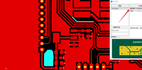
The product has only one PCB, and there is a 12MHz crystal on the board. The excessive frequencies are all multiples of 12MHz. When analyzing the screen and camera of the machine that are prone to excessive EMI radiation, it is found that the LCD-CLK is 33MHz, and the camera MCLK is 24MHz.
Through the elimination method, it is found that after removing the camera, the over-standard point still exists, and by shielding the 12MHz crystal, the over-standard point is reduced. It is judged that the 144MHz over-standard point is related to the crystal. The PCB layout is as follows:

2.Radiation generation principle
From the PCB layout, it can be seen that the 12MHz crystal is arranged at the edge of the PCB. When the product is placed in the test environment of radiation emission, the high-speed device of the tested product and the reference ground in the laboratory will form a certain capacitive coupling, generating parasitic capacitance, resulting in common-mode radiation.
The larger the parasitic capacitance, the stronger the common-mode radiation; and the parasitic capacitance is actually the electric field distribution between the crystal and the reference ground. When the voltage between the two is When the electric field is constant, the more electric field distribution there is between the two, the greater the electric field strength between the two, and the greater the parasitic capacitance. The electric field distribution of the crystal at the edge of the PCB and in the middle of the PCB is as follows:


It can be seen from the figure that when the crystal oscillator is arranged in the middle of the PCB or far away from the edge of the PCB, due to the existence of the working ground (GND) plane in the PCB, most of the electric field is controlled between the crystal oscillator and the working ground, that is, inside the PCB, and the electric field distributed to the reference ground plane is greatly reduced, resulting in reduced radiation emission.
3.Treatment measures
Move the crystal oscillator inward so that it is at least 1 cm away from the edge of the PCB, and apply copper to the surface of the PCB within 1 cm of the crystal oscillator, and connect the surface copper to the PCB ground plane through vias. The modified test result spectrum is as follows. It can be seen from the figure that the radiation emission has been significantly improved.
4.Thoughts and inspirations
The capacitive coupling between high-speed printed lines or devices and the reference ground plane will cause EMI problems, and sensitive printed lines or devices placed at the edge of the PCB will cause immunity problems.
If the design must be placed at the edge of the PCB for some other reasons, then you can lay another working ground line on the edge of the printed line and add more vias to connect this working ground line to the working ground plane.