Why Design Balanced Stackup PCBs? What Are the Advantages?
Introduction
Printed Circuit Boards (PCBs) are the backbone of modern electronics, providing mechanical support and electrical connectivity for components. As electronic devices become more complex and operate at higher frequencies, PCB design must evolve to meet performance demands. One critical aspect of advanced PCB design is the balanced stackup, which ensures signal integrity, power distribution, and mechanical stability.
This article explores the reasons for designing balanced stackup PCBs and their key advantages, including improved signal integrity, reduced electromagnetic interference (EMI), better power delivery, and enhanced manufacturability.
What Is a Balanced Stackup PCB?
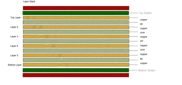
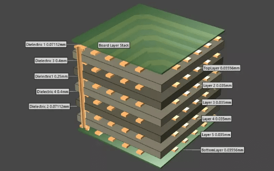
A balanced stackup refers to a PCB layer arrangement where the copper and dielectric layers are symmetrically distributed around the center of the board. This means that for every conductive layer on one side of the center, there is a corresponding layer on the opposite side with similar properties (thickness, material, and copper weight).
Example of a Balanced 8-Layer Stackup:
| Layer | Material | Purpose |
|---|---|---|
| 1 | Signal | Top Layer (Microstrip) |
| 2 | Ground | Reference Plane |
| 3 | Signal | Inner Signal Layer |
| 4 | Power | Power Plane |
| 5 | Power | Power Plane (Mirror of Layer 4) |
| 6 | Signal | Inner Signal Layer (Mirror of Layer 3) |
| 7 | Ground | Reference Plane (Mirror of Layer 2) |
| 8 | Signal | Bottom Layer (Microstrip) |
In this structure, Layers 1 & 8, 2 & 7, 3 & 6, and 4 & 5 are symmetric pairs, ensuring balance.
Why Design a Balanced Stackup PCB?
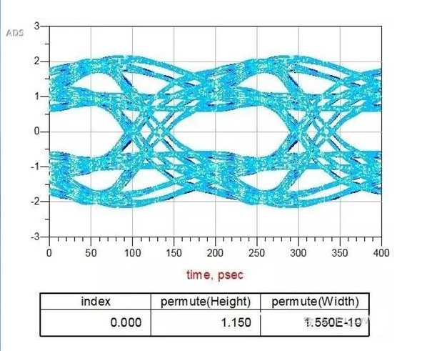
1. Improved Signal Integrity
High-speed digital and RF circuits require precise impedance control to minimize signal reflections and distortions. A balanced stackup ensures:
- Consistent impedance across differential pairs and single-ended traces.
- Reduced skew in high-speed signals (e.g., DDR, PCIe, USB).
- Minimized crosstalk due to proper shielding from adjacent ground/power planes.
Without a balanced stackup, asymmetric dielectric layers can cause impedance mismatches, leading to signal degradation.
2. Reduced Electromagnetic Interference (EMI)
A symmetric stackup helps in:
- Canceling out electromagnetic fields due to opposing current flows in mirrored layers.
- Shielding sensitive signals between ground planes, reducing radiated emissions.
- Complying with EMC/EMI regulations (e.g., FCC, CE) by minimizing noise.
Unbalanced PCBs can act as antennas, emitting unwanted radiation and failing compliance tests.
3. Better Power Distribution
A balanced power delivery network (PDN) is crucial for stable voltage supply:
- Lower power plane inductance due to closely coupled power-ground pairs.
- Reduced voltage drops (IR drop) by providing multiple low-impedance paths.
- Improved decoupling capacitor effectiveness due to shorter return paths.
An imbalanced stackup can lead to power noise, ground bounce, and unstable operation in high-current designs.
4. Enhanced Mechanical Stability
PCBs undergo thermal and mechanical stress during manufacturing and operation. A balanced stackup:
- Prevents warping and twisting during lamination (uneven copper distribution causes bending).
- Improves reliability in thermal cycling (CTE mismatch is minimized).
- Ensures even etching during fabrication, avoiding over- or under-etching.
Unbalanced designs may warp after reflow soldering, leading to assembly defects.
5. Easier Manufacturing and Lower Costs
PCB fabrication involves multiple processes (etching, drilling, plating). A balanced stackup:
- Simplifies lamination by ensuring even resin flow.
- Reduces scrap rates due to fewer warpage-related defects.
- Improves yield by minimizing impedance variations.
Unbalanced designs may require additional materials or processes, increasing costs.

Key Advantages of Balanced Stackup PCBs
| Advantage | Explanation |
|---|---|
| Improved Signal Integrity | Consistent impedance, reduced reflections, and minimized crosstalk. |
| Lower EMI Emissions | Symmetric fields cancel noise, improving EMC compliance. |
| Stable Power Delivery | Low-impedance PDN with minimized voltage fluctuations. |
| Reduced Warpage | Symmetric copper distribution prevents bending during assembly. |
| Better Manufacturability | Higher yield, fewer defects, and lower fabrication costs. |
When Is a Balanced Stackup Necessary?
Balanced stackups are particularly beneficial in:
- High-speed digital designs (DDR, PCIe, Ethernet).
- RF/microwave circuits (5G, radar, wireless comms).
- High-power applications (servers, GPUs, power electronics).
- Multi-layer HDI PCBs (smartphones, IoT devices).
For simple, low-frequency designs (e.g., two-layer Arduino boards), an unbalanced stackup may suffice.
Conclusion
A balanced stackup PCB is essential for high-performance electronics, offering superior signal integrity, reduced EMI, stable power delivery, and mechanical reliability. By ensuring symmetry in layer distribution, designers can avoid common issues like warping, noise, and impedance mismatches. As PCB technology advances toward higher speeds and densities, adopting a balanced stackup becomes not just an option but a necessity for robust, manufacturable, and high-quality circuit boards.
By understanding and implementing balanced stackups, engineers can optimize their designs for performance, compliance, and cost-effectiveness in modern electronics.