Why Does AME Need 3D PCB Structure?
Introduction
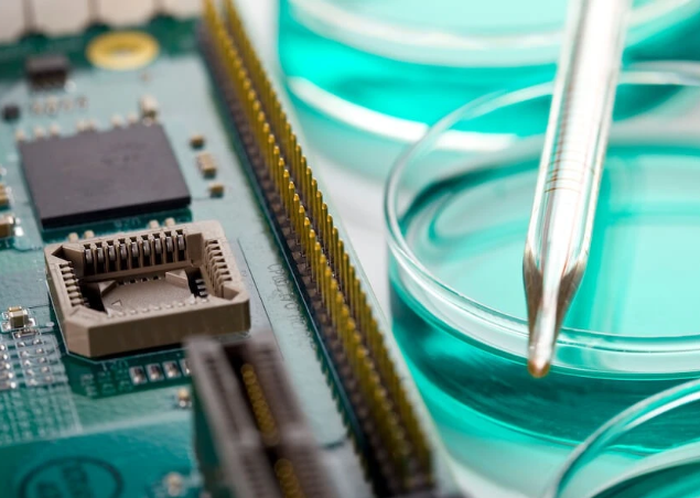
In the rapidly evolving field of Advanced Manufacturing Engineering (AME), the demand for more sophisticated, compact, and high-performance electronic systems has never been greater. As electronic devices become increasingly complex while simultaneously shrinking in size, traditional two-dimensional (2D) printed circuit board (PCB) designs are reaching their physical limitations. This has led to the emergence and growing adoption of three-dimensional (3D) PCB structures as a critical solution for next-generation electronic systems. This article explores the fundamental reasons why AME requires 3D PCB structures, examining the technological advantages, performance benefits, and future-proofing capabilities that 3D PCB designs offer to modern manufacturing engineering.
The Limitations of Traditional 2D PCB Designs
Space Constraints in Modern Electronics
The most apparent limitation of conventional 2D PCBs is their inability to efficiently utilize space in three dimensions. As electronic devices continue to shrink in size while increasing in functionality, the available surface area on a flat PCB becomes insufficient to accommodate all necessary components and their interconnections. Smartphones, wearable devices, IoT sensors, and medical implants are just a few examples where space optimization is critical, and 2D layouts simply cannot provide adequate solutions.
Signal Integrity Challenges at High Frequencies
With the rise of 5G, millimeter-wave technologies, and high-speed data transmission, maintaining signal integrity has become increasingly challenging with traditional PCB layouts. In 2D designs, long trace lengths and the need to route signals around components can lead to signal degradation, crosstalk, and electromagnetic interference (EMI) problems. These issues become more pronounced as signal frequencies continue to climb into the gigahertz range.
Thermal Management Difficulties
Modern electronic components generate significant amounts of heat, and 2D PCB structures often struggle with efficient heat dissipation. The flat nature of these boards limits the available surface area for heat sinks and makes it difficult to implement effective thermal pathways, potentially leading to performance throttling or reduced component lifespan.
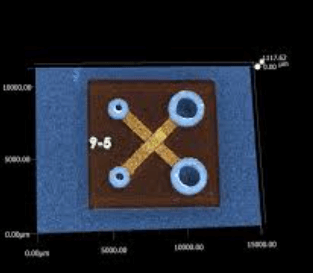
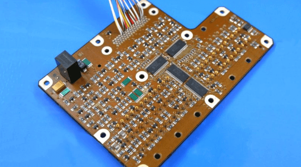
The Advantages of 3D PCB Structures
Enhanced Component Density and Miniaturization
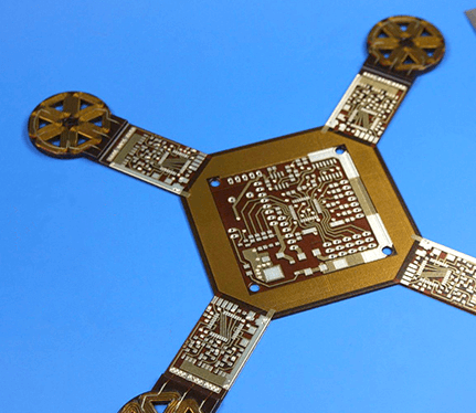
3D PCB structures allow for components to be mounted and interconnected in all three spatial dimensions, dramatically increasing the potential component density within a given footprint. This vertical integration enables:
- Stacking of multiple PCB layers
- Placement of components on both sides of boards
- Integration of components within the board structure itself
- Implementation of embedded components
This approach is particularly valuable for applications where space is at a premium, such as in aerospace, medical devices, and portable electronics.
Improved Electrical Performance
The three-dimensional nature of these PCB structures offers several electrical advantages:
- Reduced Signal Path Lengths: By allowing more direct routing between components in 3D space, signal paths can be significantly shortened, reducing latency and improving signal integrity.
- Better EMI Control: 3D structures enable more effective shielding strategies and can incorporate ground planes in three dimensions to contain electromagnetic emissions.
- Optimized Power Distribution: Three-dimensional power delivery networks can provide lower impedance paths and better decoupling capacitance placement.
Advanced Thermal Management Solutions
3D PCB structures facilitate innovative thermal management approaches:
- Vertical Heat Dissipation Paths: Heat can be conducted away from components through the Z-axis of the board structure.
- Integrated Cooling Channels: Some 3D PCB technologies allow for microfluidic cooling channels to be incorporated directly into the board.
- Improved Heat Spreader Implementation: Thermal vias and other heat spreading techniques are more effectively implemented in three dimensions.
Increased Design Flexibility
The move to 3D PCB structures provides engineers with unprecedented design freedom:
- Components can be placed based on optimal functional relationships rather than planar constraints.
- Different technologies (RF, digital, power) can be more effectively isolated while maintaining necessary interconnections.
- Mechanical and electrical design can be more tightly integrated.
Applications Driving the Need for 3D PCB in AME
Aerospace and Defense Systems
The aerospace industry demands electronics that are both highly reliable and extremely compact. 3D PCB structures enable:
- Reduced weight and volume of avionics systems
- Improved resistance to vibration and mechanical stress
- Enhanced reliability through reduced interconnection points
Medical Electronics
Medical devices, particularly implants and portable diagnostic equipment, benefit from 3D PCB technology through:
- Ultra-compact form factors
- Improved reliability in challenging environments
- Better integration with mechanical components
Automotive Electronics
Modern vehicles, especially electric and autonomous ones, require sophisticated electronics in harsh environments. 3D PCBs provide:
- Higher density for advanced driver-assistance systems (ADAS)
- Improved thermal performance for power electronics
- Better space utilization in tight vehicle packaging
High-Performance Computing
Data centers and supercomputers leverage 3D PCB technology to:
- Increase processing density
- Reduce communication latency between components
- Improve energy efficiency
Technological Enablers of 3D PCB Structures
Several key technologies have made 3D PCB structures practical for AME applications:
Advanced Manufacturing Techniques
- Embedded Component Technology: Allows passive and active components to be placed within the PCB layers.
- 3D Printing of Electronics: Enables creation of complex non-planar circuit geometries.
- Laser Direct Structuring (LDS): Permits circuit patterning on three-dimensional plastic parts.
New Materials
- High-performance dielectric materials with better thermal and electrical properties.
- Conductive inks and adhesives for vertical interconnects.
- Thermally conductive but electrically insulating materials for improved heat dissipation.
Design Tools and Simulation Software
Modern electronic design automation (EDA) tools now support:
- True 3D PCB design and visualization
- 3D electromagnetic simulation
- Thermal analysis in three dimensions
- Mechanical stress modeling
Challenges in Implementing 3D PCB Structures
While the benefits are clear, there are still challenges to widespread adoption:
Manufacturing Complexity
3D PCB structures often require:
- Specialized equipment and processes
- Tighter process controls
- New quality assurance methodologies
Higher Initial Costs
The increased complexity typically leads to:
- Higher prototyping costs
- Greater investment in manufacturing infrastructure
- Need for specialized training
Design Complexity
Engineers must adapt to:
- New design rules and constraints
- More complex verification processes
- Additional considerations for manufacturability
The Future of 3D PCB in AME
As manufacturing technologies mature and costs decrease, 3D PCB adoption is expected to accelerate across all sectors of advanced manufacturing engineering. Future developments may include:
- Hybrid 3D structures combining different technologies
- Increased integration with mechanical components
- Smart structures with embedded sensors
- Self-healing materials and structures
Conclusion
The transition from traditional 2D PCB designs to advanced 3D PCB structures represents a fundamental evolution in electronic packaging that addresses the growing demands of Advanced Manufacturing Engineering. By enabling higher component densities, improved electrical performance, better thermal management, and greater design flexibility, 3D PCB technology provides solutions to many of the challenges facing modern electronic systems. While implementation challenges remain, the benefits are driving rapid adoption across industries from consumer electronics to aerospace and medical devices. As manufacturing processes continue to advance and design tools become more sophisticated, 3D PCB structures will undoubtedly become the standard rather than the exception in AME, enabling the next generation of innovative electronic products. The question is no longer whether AME needs 3D PCB structures, but how quickly the industry can adapt to fully leverage their transformative potential.