Wire for pcb board
How to choose wire for pcb board
When designing a printed circuit board (PCB), one of the critical decisions that engineers must make is selecting the appropriate wire gauge.
This choice significantly impacts the performance, reliability, and safety of the final product. Understanding the factors that influence wire gauge selection is essential for ensuring that the PCB functions as intended under various operating conditions.
To begin with, the wire gauge, which refers to the diameter of the wire, directly affects the current-carrying capacity.
Thicker wires can carry more current without overheating, while thinner wires are suitable for lower current applications. The American Wire Gauge (AWG) system is commonly used to specify wire diameters, with lower numbers indicating thicker wires. For instance, a 12 AWG wire is thicker and can carry more current than a 24 AWG wire. Therefore, the first step in choosing the right wire gauge is to determine the maximum current that the PCB will need to handle.
In addition to current capacity, voltage drop is another crucial consideration.
As current flows through a wire, it encounters resistance, which causes a voltage drop along the length of the wire. This drop can affect the performance of the components on the PCB, especially in precision applications where maintaining a stable voltage is critical. Thicker wires have lower resistance and, consequently, lower voltage drops. Therefore, for applications requiring minimal voltage drop, selecting a thicker wire gauge is advisable.
Thermal management is another factor that cannot be overlooked.
As current flows through a wire, it generates heat due to the wire’s resistance. Excessive heat can damage the PCB and its components, leading to potential failures. Thicker wires dissipate heat more effectively than thinner ones, reducing the risk of overheating. Therefore, in high-power applications where significant heat generation is expected, opting for a thicker wire gauge is prudent.
Moreover, the physical layout of the PCB also influences wire gauge selection.
In densely packed boards with limited space, using thicker wires may not be feasible. Engineers must balance the need for adequate current-carrying capacity with the available space on the PCB. In such cases, careful planning and optimization of the PCB layout are necessary to ensure that the chosen wire gauge can be accommodated without compromising the board’s functionality.
Another aspect to consider is the mechanical strength of the wire.
Thicker wires are generally more robust and can withstand mechanical stresses better than thinner wires. This is particularly important in applications where the PCB may be subjected to vibrations or other mechanical forces. Ensuring that the wire gauge provides sufficient mechanical strength can enhance the durability and longevity of the PCB.
Furthermore, cost considerations also play a role in wire gauge selection.
Thicker wires are typically more expensive than thinner ones due to the increased material usage. Therefore, engineers must weigh the benefits of using a thicker wire gauge against the associated costs. In some cases, it may be possible to use a combination of different wire gauges to optimize both performance and cost.
In conclusion, choosing the right wire gauge for a PCB board involves a careful evaluation of multiple factors, including current-carrying capacity, voltage drop, thermal management, physical layout, mechanical strength, and cost. By considering these aspects and making informed decisions, engineers can ensure that their PCB designs meet the required performance standards and operate reliably under various conditions.
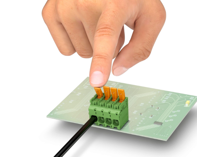
Best Practices For Soldering Wires To PCB Boards
Soldering wires to PCB boards is a fundamental skill in electronics assembly, requiring precision and adherence to best practices to ensure reliable and durable connections. The process begins with the selection of appropriate materials. High-quality solder wire, typically composed of a tin-lead alloy or a lead-free alternative, is essential. The choice of flux, which cleans and prepares the surfaces to be joined, is equally important. Rosin-based flux is commonly used for its effectiveness in removing oxidation and promoting strong solder bonds.
Before soldering, it is crucial to prepare both the wire and the PCB.
Stripping the wire to expose a clean, unoxidized section of conductor is the first step. The length of the stripped section should be just enough to make a secure connection without excess exposed wire, which could lead to shorts. Tinning the wire, which involves applying a small amount of solder to the stripped end, helps in creating a more reliable joint by ensuring that the solder flows evenly during the final soldering process.
The PCB pads or through-holes where the wire will be soldered must also be clean and free of oxidation.
This can be achieved by gently scrubbing the area with a fine abrasive or using a flux pen. Ensuring that the PCB is securely held in place, either with a PCB holder or a third-hand tool, allows for more precise soldering and reduces the risk of movement during the process.
When soldering, the correct temperature and technique are paramount.
A soldering iron with a fine tip, set to an appropriate temperature (typically between 350°C and 400°C for most solders), should be used. Applying the soldering iron to both the wire and the PCB pad simultaneously ensures that both surfaces reach the necessary temperature for the solder to flow and form a strong bond. The solder should be applied to the joint, not the iron, allowing it to flow naturally into the connection. This method helps in avoiding cold joints, which are weak and unreliable.
After the solder has flowed and formed a joint, it is important to inspect the connection.
A good solder joint should be smooth, shiny, and free of cracks or voids. If the joint appears dull or grainy, it may indicate a cold joint, which should be reworked by reheating and applying additional solder if necessary. Excess solder can be removed using desoldering braid or a solder sucker, ensuring a clean and professional finish.
Once all connections are made, cleaning the PCB to remove any residual flux is a best practice.
Flux residues can be corrosive and may lead to long-term reliability issues. Isopropyl alcohol and a soft brush can be used to clean the board, followed by a thorough inspection to ensure no solder bridges or unintended connections are present.
In conclusion, soldering wires to PCB boards requires careful preparation, the right materials, and precise technique. By following these best practices, one can achieve strong, reliable connections that ensure the longevity and performance of electronic assemblies. Attention to detail at each step of the process, from material selection to final inspection, is key to mastering this essential skill in electronics.
Common Mistakes To Avoid When Wiring PCB Boards
When wiring PCB boards, it is crucial to avoid common mistakes that can compromise the functionality and reliability of the final product. One of the most frequent errors is improper component placement. Ensuring that components are correctly positioned is essential for maintaining signal integrity and minimizing electromagnetic interference. Misplaced components can lead to increased noise and signal degradation, which can severely impact the performance of the PCB.
Another common mistake is neglecting to consider the trace width and spacing.
The width of the traces must be adequate to handle the current load without overheating, while the spacing between traces should prevent short circuits and crosstalk. Failing to adhere to these guidelines can result in overheating, which may damage the board and its components, or cause electrical shorts that can lead to malfunction.
Additionally, inadequate grounding is a prevalent issue that can cause significant problems.
A well-designed grounding system is vital for the stability and performance of the PCB. Poor grounding can lead to noise issues, signal integrity problems, and even complete failure of the board. It is essential to ensure that all components have a proper ground connection and that the ground plane is continuous and free of interruptions.
Furthermore, overlooking the importance of decoupling capacitors is a mistake that can have serious consequences.
Decoupling capacitors are used to filter out noise and provide a stable voltage supply to the components. Without them, the power supply can become unstable, leading to erratic behavior and potential damage to the components. It is important to place decoupling capacitors as close as possible to the power pins of the integrated circuits to maximize their effectiveness.
Another critical aspect to consider is the routing of high-speed signals.
High-speed signals are particularly susceptible to noise and interference, and improper routing can lead to signal integrity issues. It is essential to keep high-speed traces as short as possible and to use controlled impedance routing techniques. Additionally, avoiding sharp bends and ensuring that differential pairs are routed together can help maintain signal integrity.
Moreover, failing to perform thorough design rule checks (DRCs) is a mistake that can lead to numerous issues.
DRCs are used to verify that the PCB design adheres to the specified manufacturing and electrical rules. Skipping this step can result in design flaws that may not be immediately apparent but can cause significant problems during manufacturing or operation. It is crucial to perform comprehensive DRCs to identify and rectify any potential issues before proceeding to production.
Lastly, inadequate documentation and labeling can create confusion and errors during the assembly and testing phases.
Clear and detailed documentation, including schematics, layout files, and assembly instructions, is essential for ensuring that the PCB is assembled correctly. Proper labeling of components and test points can also facilitate troubleshooting and maintenance, reducing the likelihood of errors and improving the overall reliability of the board.
In conclusion, avoiding these common mistakes when wiring PCB boards is essential for ensuring the functionality and reliability of the final product. By paying careful attention to component placement, trace width and spacing, grounding, decoupling capacitors, high-speed signal routing, design rule checks, and documentation, designers can create robust and reliable PCBs that meet the required specifications and perform as intended.
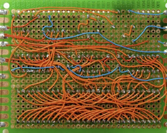
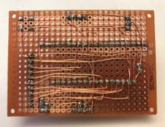
Innovative Wire Management Solutions For PCB Design
In the realm of modern electronics, the printed circuit board (PCB) stands as a cornerstone of innovation, enabling the compact and efficient assembly of electronic components. As the complexity and functionality of electronic devices continue to advance, the importance of effective wire management solutions for PCB design becomes increasingly paramount. Proper wire management not only ensures the reliability and performance of the PCB but also facilitates ease of maintenance and scalability.
One of the primary considerations in wire management for PCB design is the selection of appropriate wire types.
The choice of wire is influenced by several factors, including the electrical requirements of the circuit, the physical constraints of the PCB layout, and the environmental conditions in which the device will operate. For instance, high-frequency circuits may necessitate the use of coaxial cables to minimize signal loss and electromagnetic interference. Conversely, power distribution within the PCB might require thicker gauge wires to handle higher current loads without excessive heating.
Transitioning from wire selection to wire routing, it is essential to meticulously plan the pathways that wires will follow on the PCB.
Effective wire routing minimizes the risk of crosstalk and electromagnetic interference, which can degrade the performance of the circuit. To achieve this, designers often employ techniques such as differential pair routing, where two complementary signals are routed closely together to cancel out noise. Additionally, the use of ground planes and shielding can further enhance signal integrity by providing a stable reference point and reducing electromagnetic emissions.
Another critical aspect of wire management is the physical securing of wires to the PCB.
Loose or improperly secured wires can lead to mechanical stress and potential failure points, especially in environments subject to vibration or movement. To address this, designers may use various methods such as wire bonding, where wires are ultrasonically welded to the PCB pads, or the application of adhesive-backed cable ties and clips to anchor wires in place. These techniques not only enhance the durability of the PCB but also contribute to a cleaner and more organized layout.
Furthermore, the integration of wire management solutions into the PCB design process can significantly streamline manufacturing and assembly.
Automated wire routing and placement tools, available in advanced PCB design software, allow for precise and efficient wire management, reducing the likelihood of human error. These tools can also optimize the routing paths to minimize wire length and avoid unnecessary bends, which can introduce resistance and potential points of failure.
In addition to traditional wire management techniques, emerging technologies are offering innovative solutions to further enhance PCB design.
For example, flexible PCBs, which incorporate bendable substrates, allow for more dynamic wire routing and can accommodate complex three-dimensional shapes. This flexibility can be particularly advantageous in applications where space constraints are critical, such as in wearable electronics or compact consumer devices.
Moreover, the advent of wireless communication technologies is gradually reducing the reliance on physical wires for certain applications.
By leveraging wireless protocols such as Bluetooth, Wi-Fi, and near-field communication (NFC), designers can eliminate some of the wiring complexity, thereby simplifying the PCB layout and improving overall reliability.
In conclusion, effective wire management is a fundamental aspect of PCB design that directly impacts the performance, reliability, and manufacturability of electronic devices. By carefully selecting appropriate wire types, employing strategic routing techniques, securing wires properly, and integrating advanced design tools and technologies, designers can create robust and efficient PCBs that meet the demands of modern electronics. As technology continues to evolve, innovative wire management solutions will undoubtedly play a crucial role in shaping the future of PCB design.


