11 best high speed pcb routing practices
To meet the needs of today’s electronic products, digital circuits are getting faster and faster. High-speed design used to be a niche area of electronic products, but now most products require at least a portion of “high-speed design”. These designs require PCB designers to layout the board according to high-speed rules and requirements; for some designers, this is a new field. To this end, this article summarizes some of the most common high-speed PCB design guidelines, hoping to help your high-speed layout design.
● Prepare for high-speed PCB layout
● Device placement and PDN development in high-speed design
● Practical PCB high-speed routing suggestions
To meet the needs of today’s electronic products, digital circuits are getting faster and faster. High-speed design used to be a niche area of electronic products, but nowadays, most products require at least a portion of “high-speed design”. These designs require PCB designers to lay out the board according to high-speed rules and requirements; for some designers, this is a new field. To this end, this article summarizes some of the most common high-speed PCB design guidelines, hoping to help your high-speed layout design.
1. High-speed design settings
Before starting layout design, there are many design and database details that need to be handled in advance.
2. Schematic
While there is a lot to set up before starting a high-speed PCB layout, most people don’t give the schematic much thought. Designers should verify components, simulate circuits, and complete the design. But is the schematic itself ready for layout? A cluttered schematic can make PCB layout more difficult if the designer can’t easily understand the intent of the circuit.
For example, high-speed signal paths need to be placed in order so that designers can simulate the location of components in the layout. It is also helpful to mark areas of the design that you want the layout team to understand clearly. These include:
● Critical placement locations, and which side of the board certain components may need to be placed.
● Keep-out areas around critical components.
● High-speed routing information, including routing topology, measured lengths, and matched lengths.
● Differential pair and controlled impedance information.
3.PCB High-Speed Circuit Board Layout Design Guide
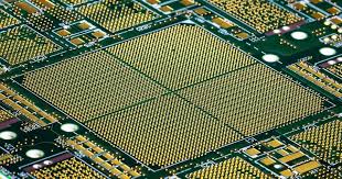
Figure 1: Dense Routing of High-Speed Circuit Boards.png
(1) Dense Routing of High-Speed Circuit Boards
(2) PCB Library
The footprint of the device used for high-speed design must be checked and verified like the PCB layout, and some additional database work will also be involved. For example, in order to ensure signal integrity in high-frequency or RF design, it may be necessary to modify the footprint used to reduce the pad size. In addition, some footprints may need to be reduced to tthe minimum size to accommodate the requirements of high-density design. However, the footprint of the device should follow the industry and manufacturer specifications as much as possible to meet the requirements of design for manufacturability (DFM). Many design tools, such as Cadence Allegro PCB Editor, can provide online library browsing functions for pulling footprint models of specified suppliers.
(3) Materials and Devices
Before starting the layout design, the materials used to manufacture the high-speed circuit board must be selected. Harsh working environments may require a more robust circuit board structure, and the physical properties of the material need to be used to calculate controlled impedance routing:
● Communicate with the manufacturer to determine whether the circuit board requires high-speed materials.
●Reinforced epoxy or PTFE materials may be better choices for high-speed and high-frequency applications.
●The dielectric constant of FR-4 may not maintain the required impedance value or cause the design to have unacceptable signal loss.
4.PCB components also need to be reviewed and confirmed by the manufacturer. Given today’s supply chain issues, it is necessary to ensure that components are available before starting the design.
(1) Board stackup
High-speed designs require a specific board stackup to achieve EMI shielding and signal integrity. The first consideration is to include a complete, continuous ground plane on the internal layers. Many boards also have multiple ground plane layers throughout the board stackup for multi-layer transmission line routing in microstrip or stripline configurations. The board stackup needs to be established in the PCB CAD database or imported from an external source. In this regard, it is very helpful if the PCB design system can communicate directly with the supplier to exchange stackup information, as shown in the video below:
(2) Design rules
PCB design systems usually have a very comprehensive set of design rules and constraints that can be set for the design. Standard PCB design uses device and net classes to specify spacing rules, trace widths, vias, and other constraints. For high-speed design, a completely new set of rules should be set, including:
● Differential pairs
● Signal paths
● Routing topology
● Measured and matched trace lengths
● Routing adjustment parameters
5.these rules can be set for each design; or in many cases, imported from another layout to reduce the designer’s workload.
(1) System parameters
The last item to set is the parameters. Parameters are very important, including display parameters such as color and fill mode, grid, routing preferences, and a series of other parameters. By managing these parameters, designers can improve their efficiency when using the tool.
PCB High-speed Circuit Board Layout Design Guide
PCB CAD system parameter setting menu for design color
Now that we have completed the settings for high-speed design, we can start laying out the circuit board.
6.PCB Design Guidelines for High-Speed Device Placement
The placement of devices in high-speed design still needs to follow the same rules as standard design placement. For balance, components should be evenly spaced around the board and design for manufacturing and testing (DFM and DFT) rules need to be followed. These include spacing of devices from other components, board features, and board edges. Devices that run at high temperatures should be grouped together to maximize the use of board area for heat dissipation, and care must be taken not to obstruct air flow over the board. Connectors and other human interface components should be placed where technicians can easily reach them, and different power supplies should be spread out from each other.
High-speed design is different in that it requires optimal signal integrity throughout the design. A major part of signal integrity depends on having a clear signal return path on the ground plane and ensuring that digital and analog circuits are separated from each other. Therefore, in addition to supporting the required trace routing, device placement must ensure clear signal return paths and circuit isolation. To accomplish this complex device placement, it is usually best to do floorplanning before placing the actual components on the board. Floorplanning helps to divide the functional partitions of the circuit without constantly moving components.
With the partitions determined, it is time to start placing the components:
● High-speed device placement guidelines
● Leave space for clear signal return paths on the reference plane.
● Allow spacing for routing channels for dense data and memory bus routing.
● Avoid placing components in areas where analog and digital circuits intersect each other.
● Component placement should ensure that high-speed signal paths are short.
● Signal paths can include multiple devices within the path, which should be placed according to the layout in the schematic.
● Analog components should be placed as close together as possible to reduce their trace lengths.
7.PCB High-Speed Circuit Board Layout Design Guide
Placement of Analog and Power Devices
As mentioned earlier, the power distribution network (PDN) should be planned at the same time as the device placement plan is made. Next, let’s learn some design recommendations for PDN.
8.Power Distribution Network (PDN) Design
In high-speed circuit boards, a well-designed PDN is critical to the final electrical performance of the board. Without a clear signal return path, the board may generate a lot of noise, resulting in erroneous signals that interfere with the normal operation of the circuit. It may also cause other signal integrity issues such as EMI and ground bounce. Return signals that do not find a clear return path on the reference plane may eventually couple to any return path they can find, including other traces. This unintentional coupling will generate common-mode currents, which may generate electromagnetic radiation and bring additional noise.
9.To avoid these problems, here are some PDN design recommendations:
● Use a continuous ground plane and do not split the ground plane
● Use device placement partitions to separate digital and analog circuits instead of splitting the ground plane.
● When routing high-speed transmission lines, make sure they have a clear signal return path on the adjacent ground plane. At higher speeds and frequencies, return paths will naturally form around the traces, so they are easy to plan.
● Be cautious about board features that may block the ground plane
● Too many vias, board cutouts, or other obstacles in a concentrated area will disrupt the clear return path on the reference plane.
● Avoid routing high-speed transmission lines in locations with gaps adjacent to the ground plane.
High-pin-count, high-density devices with multiple power connections
● Processors, memory, and other high-pin-count, high-density devices use many power pins to meet their huge power requirements.
● Each of these connections requires a bypass capacitor as close to the power pin as possible for optimal power filtering.
10.PCB High-speed Circuit Board Layout Design Guidelines
Example of high-speed routing, you can see that the routing has been adjusted
Once the network connections and PDNs of the board are optimally configured, you can start routing.
11.High-speed routing tips
When the devices on the board are arranged properly, the design will have a basic template that indicates how the routing should be arranged. However, it should be noted that we will most likely still have to move components to improve and adjust the routing – just like in any PCB design.
12.High-speed routing guidelines
● Make sure to fully follow the design rules and constraints for line length, matching length, width, spacing, layers, impedance-controlled routing parameters, differential pairs, routing adjustments, and via assignments.
● Set any necessary area rules based on unique routing needs and leave no-routing areas.
● In addition to specific routing topologies and measured lengths, try to keep routing as short and direct as possible.
● Do not route through gaps or breaks in the ground plane. This can disrupt the signal’s clear return path and potentially cause signal integrity issues discussed earlier.
● When routing high-speed signals, ensure they have a clear signal return path on the adjacent ground plane.
● For sensitive signals such as clock lines and differential pairs, ensure they have additional clearance from other routing, typically three times the standard trace width.
● Ensure that high-speed transmission lines are routed on their assigned layers to ensure their return path on the adjacent reference plane.
● Avoid changing layer properties with high-speed transmission lines, but if you must do so, try to keep them adjacent to the same ground plane to achieve a signal return path. If the layer transition is farther than the layer pair, use a ground via next to the signal via as a transition for the return path.
● Be cautious with high-speed transmission lines that run parallel to each other as they can create crosstalk.
● Pay attention to the vertical crosstalk between layers, which may be smaller than two traces side by side on the same layer.
● Use wider traces in analog routing.
● Choose a wider grid to place vias and plan via escapes for the maximum number of routing channels.
● Minimize the use of vias to reduce inductance, or use blind, buried or microvias.
● Be careful not to block the return path on the ground plane in areas with dense scattered vias.
The design guidelines for high-speed PCBs listed in this article are far from exhaustive, but they are enough to help us get started with high-speed PCB design. In addition, remember to make full use of the functions of CAD tools. In addition to the design rules and constraints mentioned above, Cadence PCB design tools have many other efficient functions to help high-speed design, such as:
● Dynamic backdrill: Backdrill information follows the design and updates in real time. After the design is adjusted, there is no need to manually update the backdrill information.
● Microvia check: Set design rules related to laser holes to ensure high-quality delivery of HDI design.
● Parameterized high-speed structure:
● No need to tediously select high-speed structure elements, just input parameters to generate the required high-speed structure;
● In the design, use high-speed structure like vias (replace, set in Constraint Manager).
● 3D Canvas: Let designers see the PCB entity, and what is displayed in front of them is the assembled PCB.
● DFM/DFA design: Set different DFM/DFA rules in different areas.
● Allegro Constraint Compiler: Convert design guidelines into design rules, realize the same source of rules, and help designers reuse rules quickly and accurately.