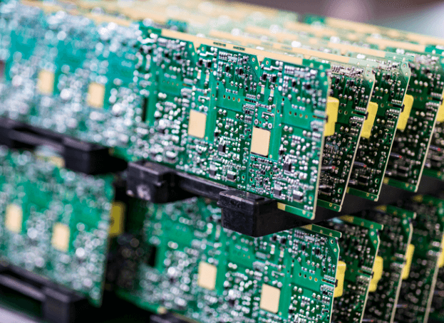
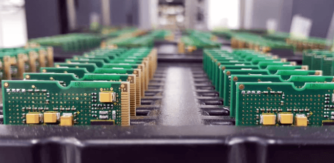
Printed circuit board manufacture
systems use high-resolution cameras and sophisticated algorithms to inspect PCBs for defects during various stages of the manufacturing process. This technology ensures that any issues are detected and corrected early, significantly reducing the likelihood of defective products reaching the market. Moreover, AOI systems contribute to higher yields and lower production costs by minimizing the need for manual inspection and rework.
The integration of advanced manufacturing techniques such as additive manufacturing, also known as 3D printing, has further revolutionized PCB production.
Additive manufacturing allows for the creation of complex, multi-layered PCBs with intricate geometries that would be challenging or impossible to achieve using traditional subtractive methods. This technology not only enables greater design flexibility but also reduces material waste and shortens production lead times. As a result, manufacturers can quickly prototype and iterate on new designs, accelerating the development of innovative electronic products.
Environmental considerations have also played a significant role in shaping modern PCB manufacturing practices.
The industry has increasingly adopted eco-friendly processes and materials to minimize its environmental impact. For instance, the use of lead-free solder and halogen-free laminates has become more widespread, reducing the release of harmful substances during production and disposal. Additionally, advancements in recycling technologies have made it easier to recover valuable materials from end-of-life PCBs, promoting a more sustainable approach to electronic waste management.
Furthermore, the advent of Industry 4.0 and the Internet of Things (IoT) has introduced new opportunities for enhancing PCB manufacturing.
Smart factories equipped with interconnected machinery and sensors can collect and analyze vast amounts of data in real-time, enabling manufacturers to optimize production processes, improve quality control, and reduce downtime. This data-driven approach not only enhances operational efficiency but also allows for more agile and responsive manufacturing, better aligning with the dynamic demands of the market.
In conclusion, the advancements in PCB manufacturing technology have significantly transformed the industry, leading to higher performance, greater efficiency, and reduced environmental impact. The adoption of advanced materials, innovative manufacturing techniques, and smart factory solutions has enabled manufacturers to meet the growing demands for more sophisticated and reliable electronic devices. As technology continues to evolve, it is likely that PCB manufacturing will continue to see further innovations, driving the next generation of electronic products.
The Importance Of Quality Control In PCB Production
In the realm of electronics, the printed circuit board (PCB) serves as the backbone of virtually all electronic devices. The manufacture of PCBs is a complex process that demands precision and meticulous attention to detail. One of the most critical aspects of this process is quality control, which ensures that the final product meets the required standards and functions as intended. The importance of quality control in PCB production cannot be overstated, as it directly impacts the reliability, performance, and longevity of electronic devices.
To begin with, quality control in PCB production involves a series of systematic procedures designed to detect and rectify defects at various stages of the manufacturing process.
This begins with the inspection of raw materials, such as copper-clad laminates and solder masks, to ensure they meet the specified quality standards. Any deviation from these standards can lead to significant issues down the line, including short circuits, signal loss, and even complete device failure. By implementing rigorous quality checks at this initial stage, manufacturers can prevent such problems from arising.
As the manufacturing process progresses, quality control measures become even more critical.
During the etching process, for instance, precision is paramount to ensure that the copper traces are accurately formed. Any discrepancies in the etching process can result in faulty connections, which can compromise the functionality of the entire PCB. To mitigate this risk, manufacturers employ advanced inspection techniques, such as automated optical inspection (AOI) and X-ray inspection, to detect and correct any defects in the copper traces.
Furthermore, the soldering process, which involves attaching electronic components to the PCB, is another crucial stage where quality control plays a vital role.
Poor soldering can lead to weak connections, which can cause intermittent failures or complete breakdowns of the electronic device. To ensure the integrity of solder joints, manufacturers use techniques such as X-ray inspection and in-circuit testing (ICT) to verify the quality of the soldering process. These methods help identify any potential issues, such as cold solder joints or insufficient solder, allowing for timely corrective actions.
In addition to these specific stages, overall quality control in PCB production also encompasses environmental and regulatory compliance.
Manufacturers must adhere to stringent industry standards, such as IPC-A-600 and IPC-6012, which define the acceptable levels of quality and performance for PCBs. Compliance with these standards not only ensures the reliability of the final product but also enhances the manufacturer’s reputation and credibility in the market.
Moreover, the implementation of robust quality control measures in PCB production has significant economic implications.
Defective PCBs can lead to costly recalls, repairs, and replacements, which can severely impact a company’s bottom line. By investing in comprehensive quality control processes, manufacturers can minimize the risk of defects and reduce the associated costs. This, in turn, leads to increased customer satisfaction and loyalty, as consumers are more likely to trust and purchase products from manufacturers known for their high-quality standards.
In conclusion, quality control is an indispensable aspect of PCB production that ensures the reliability, performance, and longevity of electronic devices.
Through meticulous inspection and testing at various stages of the manufacturing process, manufacturers can detect and rectify defects, adhere to industry standards, and maintain their reputation in the market. The economic benefits of robust quality control measures further underscore their importance, making them a critical component of successful PCB production.
Environmental Impact Of PCB Manufacturing And How To Mitigate It
The environmental impact of printed circuit board (PCB) manufacturing is a significant concern in the electronics industry. The process involves various stages, each contributing to environmental degradation through the consumption of resources and the generation of waste. To understand the full scope of this impact, it is essential to examine the materials and processes involved in PCB production, as well as the potential strategies for mitigating these effects.
PCB manufacturing begins with the selection of raw materials, primarily copper and fiberglass, which are both resource-intensive to produce.
The extraction and processing of these materials result in substantial energy consumption and greenhouse gas emissions. Additionally, the use of chemicals such as etchants, solvents, and plating solutions in the manufacturing process poses a risk to both human health and the environment. These chemicals can lead to soil and water contamination if not properly managed, further exacerbating the environmental footprint of PCB production.
Moreover, the manufacturing process generates a considerable amount of waste, including scrap materials, defective boards, and chemical by-products. The disposal of these wastes presents another environmental challenge, as improper handling can lead to the release of hazardous substances into the environment. This not only affects ecosystems but also poses a risk to public health.
To mitigate the environmental impact of PCB manufacturing, several strategies can be employed.
One effective approach is the adoption of cleaner production techniques. By optimizing the use of raw materials and reducing waste generation, manufacturers can minimize their environmental footprint. For instance, implementing closed-loop systems for chemical use can significantly reduce the amount of hazardous waste produced. These systems allow for the recycling and reuse of chemicals, thereby decreasing the need for fresh inputs and reducing the potential for environmental contamination.
Another important strategy is the development and use of environmentally friendly materials.
Researchers are exploring alternatives to traditional materials, such as biodegradable substrates and non-toxic chemicals, which can help reduce the environmental impact of PCB production. By transitioning to these greener materials, manufacturers can lessen their reliance on resource-intensive and hazardous substances, thereby mitigating their overall environmental footprint.
Energy efficiency is also a critical factor in reducing the environmental impact of PCB manufacturing.
By investing in energy-efficient technologies and practices, manufacturers can lower their energy consumption and associated greenhouse gas emissions. This can be achieved through the use of energy-efficient equipment, process optimization, and the implementation of renewable energy sources. For example, solar panels and wind turbines can provide clean energy for manufacturing facilities, reducing their dependence on fossil fuels and decreasing their carbon footprint.
Furthermore, proper waste management practices are essential in mitigating the environmental impact of PCB manufacturing.
This includes the safe disposal of hazardous waste, as well as the recycling and recovery of valuable materials from scrap boards. By implementing comprehensive waste management programs, manufacturers can ensure that waste is handled responsibly, minimizing the risk of environmental contamination.
In conclusion, the environmental impact of PCB manufacturing is a multifaceted issue that requires a combination of strategies to address effectively. By adopting cleaner production techniques, using environmentally friendly materials, improving energy efficiency, and implementing proper waste management practices, manufacturers can significantly reduce their environmental footprint. These efforts not only benefit the environment but also contribute to the sustainability of the electronics industry as a whole. As the demand for electronic devices continues to grow, it is imperative that the industry takes proactive steps to mitigate its environmental impact and promote a more sustainable future.
Trends In Flexible And Rigid-Flex PCB Design
The landscape of printed circuit board (PCB) manufacture has evolved significantly over the years, with notable advancements in both flexible and rigid-flex PCB design. These innovations are driven by the increasing demand for more compact, efficient, and versatile electronic devices. As technology continues to progress, the trends in flexible and rigid-flex PCB design are shaping the future of electronics, offering numerous benefits and addressing various challenges.
One of the most prominent trends in flexible PCB design is the push towards miniaturization.
As electronic devices become smaller and more portable, the need for compact and lightweight PCBs has grown. Flexible PCBs, with their ability to bend and conform to different shapes, are ideal for applications where space is at a premium. This trend is particularly evident in the consumer electronics industry, where devices such as smartphones, wearables, and medical implants require highly compact and efficient circuitry. The use of flexible PCBs in these applications not only saves space but also enhances the durability and reliability of the devices.
In addition to miniaturization, there is a growing emphasis on the integration of advanced materials in flexible PCB design.
Traditional materials such as polyimide and polyester are being supplemented with new, innovative materials that offer improved performance characteristics. For instance, liquid crystal polymer (LCP) and polytetrafluoroethylene (PTFE) are gaining popularity due to their excellent thermal stability, low dielectric constant, and high-frequency performance. These materials enable the development of flexible PCBs that can operate in more demanding environments and support higher data transmission rates, making them suitable for applications in telecommunications, aerospace, and automotive industries.
Transitioning to rigid-flex PCB design, one of the key trends is the increasing complexity of designs.
Rigid-flex PCBs combine the best of both worlds, offering the mechanical stability of rigid PCBs and the flexibility of flexible PCBs. This hybrid approach allows for more intricate and compact designs, which are essential for modern electronic devices. The ability to integrate multiple rigid and flexible layers within a single PCB enables designers to create more sophisticated and multifunctional circuits. This trend is particularly relevant in the development of advanced medical devices, military equipment, and industrial automation systems, where reliability and performance are paramount.
Another significant trend in rigid-flex PCB design is the focus on improving manufacturing processes.
As the demand for rigid-flex PCBs grows, manufacturers are investing in advanced fabrication techniques to enhance production efficiency and quality. Techniques such as laser drilling, precision etching, and automated optical inspection are being increasingly adopted to ensure the accuracy and consistency of rigid-flex PCBs. These advancements not only reduce production costs but also minimize the risk of defects, leading to higher yields and better overall product performance.
Furthermore, the trend towards environmental sustainability is influencing both flexible and rigid-flex PCB design.
Manufacturers are exploring eco-friendly materials and processes to reduce the environmental impact of PCB production. For example, the use of lead-free solder and halogen-free laminates is becoming more common, in line with global regulations and industry standards. Additionally, efforts are being made to improve the recyclability of PCBs, ensuring that electronic waste is managed more effectively.
In conclusion, the trends in flexible and rigid-flex PCB design reflect the ongoing advancements in technology and the evolving needs of various industries. The push towards miniaturization, the integration of advanced materials, the increasing complexity of designs, the improvement of manufacturing processes, and the focus on environmental sustainability are all shaping the future of PCB manufacture. As these trends continue to develop, they will undoubtedly lead to more innovative and efficient electronic devices, driving progress across multiple sectors.