Advanced pcb design
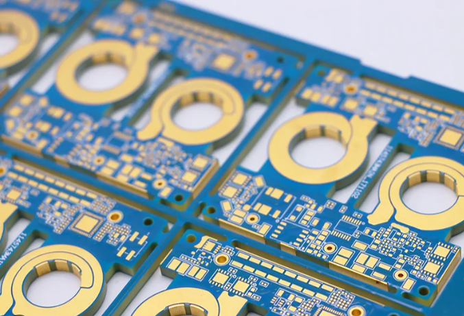
Innovations In High-Density Interconnect (HDI) PCB Design
In the rapidly evolving landscape of electronics, the demand for more compact, efficient, and powerful devices has driven significant advancements in printed circuit board (PCB) design. Among these innovations,
High-Density Interconnect (HDI) technology stands out as a pivotal development, enabling the creation of smaller, faster, and more efficient electronic devices.
As the name suggests, HDI PCBs are characterized by a higher density of interconnections compared to traditional PCBs, achieved through the use of finer lines and spaces, smaller vias, and capture pads. This technology is particularly beneficial in applications where space is at a premium, such as in smartphones, tablets, and other portable electronic devices.
One of the key innovations in HDI PCB design is the use of microvias, which are significantly smaller than conventional vias.
Microvias allow for more interconnections in a given area, thereby increasing the routing density of the PCB. This is particularly advantageous in multi-layer PCBs, where space is limited and the need for efficient routing is paramount. The use of microvias not only enhances the electrical performance of the PCB by reducing signal loss and improving signal integrity but also contributes to the overall miniaturization of electronic devices.
In addition to microvias, the incorporation of advanced materials has played a crucial role in the evolution of HDI PCB design.
Traditional PCBs are typically made from materials such as FR-4, which, while cost-effective, may not always meet the performance requirements of high-speed and high-frequency applications. In contrast, HDI PCBs often utilize advanced materials like polyimide and liquid crystal polymer, which offer superior thermal and electrical properties. These materials enable the PCBs to withstand higher temperatures and frequencies, making them ideal for use in cutting-edge applications such as 5G technology and advanced computing systems.
Moreover, the advent of laser drilling technology has revolutionized the manufacturing process of HDI PCBs.
Laser drilling allows for the precise creation of microvias, which are essential for achieving the high interconnect density characteristic of HDI designs. This technology not only improves the accuracy and efficiency of the manufacturing process but also reduces the risk of defects, thereby enhancing the reliability and performance of the final product. As a result, manufacturers can produce more complex and sophisticated PCBs that meet the stringent demands of modern electronic devices.
Furthermore, the integration of advanced design software has facilitated the development of more intricate HDI PCB layouts.
These software tools enable designers to simulate and optimize the performance of their designs before they are physically manufactured, thereby reducing the likelihood of errors and ensuring that the final product meets the desired specifications. This capability is particularly important in the context of HDI PCBs, where the complexity of the design can pose significant challenges.
In conclusion, the innovations in High-Density Interconnect PCB design have been instrumental in advancing the capabilities of modern electronic devices.
Through the use of microvias, advanced materials, laser drilling technology, and sophisticated design software, HDI PCBs offer a level of performance and miniaturization that was previously unattainable. As technology continues to evolve, it is likely that HDI PCB design will play an increasingly important role in shaping the future of electronics, enabling the development of even more compact, efficient, and powerful devices.
Techniques For Effective Thermal Management In PCB Layout
In the realm of advanced printed circuit board (PCB) design, effective thermal management is a critical consideration that can significantly impact the performance and reliability of electronic devices. As electronic components become increasingly powerful and compact, the challenge of dissipating heat efficiently becomes more pronounced. Therefore, employing effective thermal management techniques in PCB layout is essential to ensure optimal functionality and longevity of the device.
One fundamental technique for managing heat in PCB design is the strategic placement of components.
By positioning heat-generating components, such as processors and power transistors, away from heat-sensitive elements, designers can minimize the risk of thermal interference. Additionally, placing these components near the edges of the PCB can facilitate better heat dissipation, as it allows for more efficient airflow and heat transfer to the surrounding environment. This approach not only aids in maintaining a balanced thermal profile across the board but also enhances the overall thermal performance of the system.
Moreover, the use of thermal vias is another effective strategy in PCB thermal management.
Thermal vias are small, plated holes that connect the top and bottom layers of a PCB, allowing heat to be conducted away from hot spots. By incorporating an array of thermal vias beneath heat-generating components, designers can create a pathway for heat to be transferred to a larger area, thereby reducing localized temperature rise. This technique is particularly beneficial in multi-layer PCBs, where heat can be effectively distributed across different layers, enhancing the board’s ability to dissipate heat.
In addition to component placement and thermal vias, the selection of appropriate materials plays a pivotal role in thermal management.
High thermal conductivity materials, such as copper, are commonly used in PCB design to facilitate efficient heat transfer. The thickness of copper layers can be adjusted to accommodate the thermal requirements of the design, with thicker layers providing better heat dissipation capabilities. Furthermore, the use of thermal interface materials (TIMs) between components and the PCB can improve thermal conductivity, ensuring that heat is effectively transferred away from critical areas.
Another technique that can be employed is the use of heat sinks and thermal pads.
Heat sinks are passive heat exchangers that absorb and dissipate heat from components, while thermal pads provide a conductive interface between the component and the heat sink. By selecting the appropriate size and material for heat sinks, designers can enhance the thermal performance of the PCB, ensuring that components operate within their specified temperature ranges. This approach is particularly useful in high-power applications, where efficient heat dissipation is crucial to prevent overheating and potential failure.
Furthermore, the implementation of thermal simulations during the design phase can provide valuable insights into the thermal behavior of the PCB.
By using simulation tools, designers can model the heat distribution across the board and identify potential hot spots. This allows for the optimization of component placement, material selection, and cooling strategies before the physical prototype is developed. Consequently, thermal simulations can significantly reduce the risk of thermal issues arising during the testing and production stages.
In conclusion, effective thermal management in PCB layout is a multifaceted challenge that requires a combination of strategic component placement, the use of thermal vias, appropriate material selection, and the integration of heat sinks and thermal pads. By employing these techniques, designers can ensure that electronic devices operate efficiently and reliably, even under demanding conditions. As technology continues to advance, the importance of robust thermal management strategies in PCB design will only become more pronounced, underscoring the need for continuous innovation and adaptation in this critical aspect of electronic design.
The Role Of Signal Integrity In Advanced PCB Design
In the realm of advanced printed circuit board (PCB) design, signal integrity plays a pivotal role in ensuring the optimal performance and reliability of electronic devices. As technology continues to evolve, the demand for faster, more efficient, and compact electronic systems has intensified, making signal integrity a critical consideration in the design process. Signal integrity refers to the quality and reliability of electrical signals as they travel through the PCB, and it encompasses a range of factors including signal timing, noise, and electromagnetic interference.
To begin with, the importance of signal integrity in advanced PCB design cannot be overstated.
As electronic devices become more complex, the density of components on a PCB increases, leading to potential issues such as crosstalk, reflections, and impedance mismatches. These issues can degrade signal quality, resulting in data errors, increased power consumption, and even complete system failure. Therefore, maintaining signal integrity is essential to ensure that signals are transmitted accurately and efficiently across the PCB.
One of the primary challenges in maintaining signal integrity is managing the high-speed signals that are prevalent in modern electronic systems.
High-speed signals are particularly susceptible to degradation due to their sensitivity to various forms of interference. To address this, designers must carefully consider the layout of the PCB, paying close attention to trace routing, layer stack-up, and component placement. For instance, minimizing the length of signal traces and ensuring proper impedance matching can significantly reduce signal degradation. Additionally, using differential signaling and controlled impedance traces can help mitigate the effects of noise and crosstalk.
Moreover, the choice of materials used in PCB fabrication also plays a crucial role in signal integrity.
Advanced materials with low dielectric constants and low loss tangents are preferred as they help reduce signal attenuation and dispersion. Furthermore, the use of high-quality connectors and vias is essential to maintain signal integrity across different layers of the PCB. By selecting appropriate materials and components, designers can enhance the overall performance and reliability of the PCB.
In addition to physical design considerations, simulation and analysis tools are indispensable in ensuring signal integrity.
These tools allow designers to model and predict the behavior of signals within the PCB, enabling them to identify potential issues and optimize the design before fabrication. Signal integrity simulation tools can analyze various parameters such as signal rise time, eye diagrams, and jitter, providing valuable insights into the performance of the PCB. By leveraging these tools, designers can make informed decisions and implement necessary design modifications to enhance signal integrity.
Furthermore, as the industry moves towards higher frequencies and faster data rates, the role of signal integrity becomes even more pronounced. Emerging technologies such as 5G, IoT, and high-performance computing demand PCBs that can handle high-speed data transmission with minimal signal degradation. Consequently, designers must stay abreast of the latest advancements in signal integrity techniques and tools to meet these evolving requirements.
In conclusion, signal integrity is a fundamental aspect of advanced PCB design that directly impacts the performance and reliability of electronic systems. By addressing the challenges associated with high-speed signals, selecting appropriate materials, and utilizing simulation tools, designers can ensure that their PCBs meet the stringent demands of modern technology. As electronic devices continue to advance, the emphasis on signal integrity will only grow, underscoring its critical role in the future of PCB design.
Leveraging AI And Machine Learning In PCB Design Automation
In the rapidly evolving field of electronics, the design and development of printed circuit boards (PCBs) have become increasingly complex, necessitating innovative approaches to streamline the process.
One such approach is the integration of artificial intelligence (AI) and machine learning (ML) into PCB design automation.
This integration not only enhances the efficiency of the design process but also significantly improves the quality and performance of the final product. As the demand for more sophisticated electronic devices grows, leveraging AI and ML in PCB design has become a pivotal strategy for engineers and designers.
To begin with, AI and ML technologies offer substantial benefits in the optimization of PCB layouts.
Traditional design methods often involve iterative processes that can be time-consuming and prone to human error. However, AI algorithms can analyze vast amounts of data to identify optimal design patterns and configurations. By learning from previous designs and outcomes, these algorithms can predict potential issues and suggest improvements, thereby reducing the need for multiple design iterations. This predictive capability not only accelerates the design process but also enhances the reliability of the final product.
Moreover, machine learning models can be employed to automate the component placement and routing processes, which are critical aspects of PCB design.
These models can evaluate numerous design parameters and constraints to determine the most efficient placement of components and routing of connections. By doing so, they minimize signal interference and power consumption, which are crucial for the performance and longevity of electronic devices. Additionally, AI-driven tools can simulate various environmental conditions and stress factors, allowing designers to assess the robustness of their designs under different scenarios. This proactive approach to design validation ensures that potential failures are identified and addressed early in the development cycle.
Furthermore, the integration of AI and ML in PCB design automation facilitates enhanced collaboration among design teams.
AI-powered platforms can provide real-time feedback and suggestions, enabling designers to make informed decisions quickly. This collaborative environment fosters innovation and creativity, as team members can experiment with different design approaches and receive immediate insights into their feasibility and impact. Consequently, this leads to more innovative and efficient designs that meet the ever-increasing demands of the electronics market.
In addition to improving design efficiency and collaboration, AI and ML also contribute to cost reduction in PCB manufacturing.
By optimizing design processes and minimizing errors, these technologies reduce the need for costly prototyping and rework. Furthermore, AI-driven analytics can predict manufacturing challenges and suggest adjustments to the design, ensuring a smoother transition from design to production. This predictive capability not only saves time and resources but also enhances the overall quality of the manufactured PCBs.
In conclusion, the integration of AI and machine learning into PCB design automation represents a significant advancement in the field of electronics. By optimizing design processes, enhancing collaboration, and reducing costs, these technologies are transforming the way PCBs are designed and manufactured. As the complexity of electronic devices continues to increase, the role of AI and ML in PCB design will undoubtedly become even more critical. Embracing these technologies will enable designers and engineers to meet the challenges of the future, delivering innovative and high-performance electronic solutions to the market.