Hdi pcb structure
Understanding The Layers Of HDI PCB Structure
High-Density Interconnect (HDI) printed circuit boards (PCBs) represent a significant advancement in the field of electronics, offering enhanced performance and miniaturization capabilities. Understanding the layers of HDI PCB structure is crucial for appreciating how these sophisticated boards meet the demands of modern electronic devices. At the core of HDI technology is the ability to incorporate more components in a smaller area, which is achieved through a complex layering process that distinguishes HDI PCBs from traditional ones.
To begin with, the fundamental structure of an HDI PCB involves multiple layers that are intricately interconnected.
These layers typically include a combination of core layers and build-up layers. The core layer serves as the foundational substrate, providing mechanical support and housing the primary circuitry. It is usually made from materials such as FR-4, a composite of woven fiberglass cloth with an epoxy resin binder, which offers a balance of strength and thermal resistance. On top of this core, build-up layers are added, which are essential for increasing the circuit density.
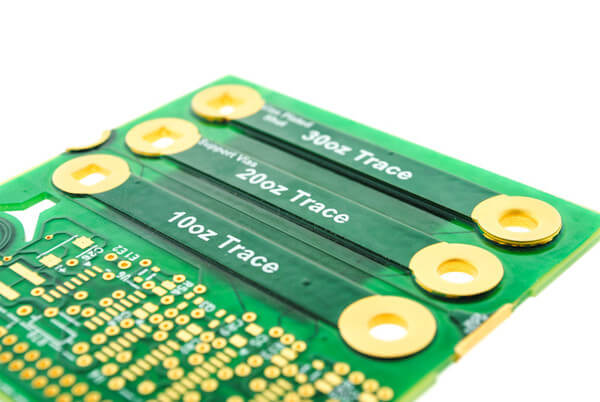
Transitioning to the build-up layers, these are characterized by their use of microvias, which are small-diameter vias that connect different layers of the PCB.
Unlike traditional through-hole vias, microvias are drilled using laser technology, allowing for precise and compact interconnections. This capability is pivotal in HDI PCBs, as it enables the creation of finer lines and spaces, thus accommodating more components in a limited space. The use of microvias not only enhances the electrical performance by reducing signal loss and inductance but also contributes to the overall reliability of the board.
Furthermore, the layering process in HDI PCBs often involves sequential lamination, a technique that allows for the addition of multiple build-up layers.
This process begins with the lamination of the core layer, followed by the application of dielectric materials and copper foils to form additional layers. Each layer is carefully aligned and bonded under heat and pressure, ensuring a robust and cohesive structure. Sequential lamination is particularly advantageous in HDI PCBs as it facilitates the integration of complex circuitry without compromising the board’s integrity.
In addition to the physical layering, the HDI PCB structure is also defined by its electrical characteristics.
The use of advanced materials and precise manufacturing techniques results in improved signal integrity and reduced electromagnetic interference. This is crucial for high-speed applications where signal clarity and timing are paramount. Moreover, the compact nature of HDI PCBs allows for shorter signal paths, which further enhances performance by minimizing latency and power consumption.
As we delve deeper into the intricacies of HDI PCB structure, it becomes evident that the design and manufacturing processes are highly specialized.
Engineers must consider various factors such as thermal management, impedance control, and manufacturability to ensure optimal performance. The choice of materials, the configuration of layers, and the implementation of microvias all play a critical role in defining the capabilities of the final product.
In conclusion, the layers of HDI PCB structure are a testament to the advancements in electronic design and manufacturing. By leveraging sophisticated layering techniques and materials, HDI PCBs offer unparalleled performance and miniaturization, meeting the ever-evolving demands of modern technology. Understanding these layers provides valuable insight into how HDI PCBs continue to revolutionize the electronics industry, paving the way for more compact, efficient, and powerful devices.

Advantages Of HDI PCB Structure In Modern Electronics
High-Density Interconnect (HDI) Printed Circuit Boards (PCBs) have become a cornerstone in the advancement of modern electronics, offering a multitude of advantages that cater to the ever-evolving demands of technology. As electronic devices continue to shrink in size while increasing in functionality, the need for more efficient and compact circuit board designs has become paramount. HDI PCBs address this need by providing a structure that supports higher wiring density, improved performance, and enhanced reliability, making them an indispensable component in the electronics industry.
One of the primary advantages of HDI PCB structures is their ability to accommodate more components in a smaller area.
This is achieved through the use of microvias, blind vias, and buried vias, which allow for more interconnections between layers without compromising the board’s integrity. Consequently, HDI PCBs enable the design of smaller, lighter, and more compact devices, which is particularly beneficial in the production of smartphones, tablets, and other portable electronics. The reduction in size does not only contribute to the aesthetic appeal of these devices but also enhances their portability and user convenience.
In addition to size reduction, HDI PCBs offer significant improvements in electrical performance.
The shorter signal paths made possible by the dense interconnects reduce signal loss and electromagnetic interference, leading to faster signal transmission and improved overall performance. This is crucial in high-speed applications where even the slightest delay can impact functionality. Moreover, the enhanced electrical performance of HDI PCBs supports the integration of advanced features and capabilities, such as high-resolution displays and faster processing speeds, which are essential in meeting consumer expectations for cutting-edge technology.
Another notable advantage of HDI PCB structures is their contribution to increased reliability and durability.
The use of advanced materials and manufacturing techniques in HDI PCBs results in boards that can withstand higher thermal and mechanical stresses. This is particularly important in applications where devices are subjected to harsh environments or continuous operation, such as in automotive and industrial electronics. The robust nature of HDI PCBs ensures that devices maintain their performance and longevity, reducing the likelihood of failure and the need for frequent repairs or replacements.
Furthermore, HDI PCBs facilitate greater design flexibility, allowing engineers to explore innovative solutions and optimize the functionality of electronic devices.
The ability to incorporate more layers and interconnections without increasing the board’s size opens up new possibilities for complex circuit designs. This flexibility is instrumental in the development of multifunctional devices that cater to diverse consumer needs, from wearable technology to sophisticated medical equipment.
In conclusion, the advantages of HDI PCB structures in modern electronics are manifold, encompassing size reduction, improved electrical performance, enhanced reliability, and increased design flexibility. As technology continues to advance, the demand for more efficient and compact electronic devices will only grow, further solidifying the role of HDI PCBs in the industry. By enabling the development of smaller, faster, and more reliable devices, HDI PCBs not only meet current technological demands but also pave the way for future innovations. As such, they remain a critical component in the ongoing evolution of modern electronics, driving progress and shaping the future of technology.
Design Considerations For HDI PCB Structure
High-Density Interconnect (HDI) printed circuit boards (PCBs) have become a cornerstone in modern electronics, offering enhanced performance and miniaturization capabilities. As the demand for more compact and efficient electronic devices grows, understanding the design considerations for HDI PCB structures becomes increasingly crucial. These considerations are pivotal in ensuring that the final product meets the desired specifications and functions optimally.
To begin with, one of the primary design considerations for HDI PCBs is the selection of materials.
The choice of substrate material significantly impacts the board’s performance, reliability, and cost. Common materials include FR-4, polyimide, and Rogers, each offering distinct advantages. For instance, FR-4 is widely used due to its cost-effectiveness and good electrical insulation properties, while polyimide is preferred for its flexibility and thermal stability. The material selection should align with the specific requirements of the application, such as thermal management, mechanical strength, and signal integrity.
Another critical aspect is the layer stack-up configuration.
HDI PCBs typically feature multiple layers, which allow for more complex routing and increased component density. The stack-up design must be carefully planned to optimize signal integrity and minimize electromagnetic interference (EMI). This involves determining the number of layers, the arrangement of power and ground planes, and the placement of signal traces. A well-designed stack-up can significantly enhance the board’s performance by reducing crosstalk and ensuring efficient power distribution.
Furthermore, the use of microvias is a defining characteristic of HDI PCBs.
These small vias enable connections between layers and contribute to the board’s high-density capabilities. The design of microvias requires precision, as their size and placement can affect the board’s reliability and manufacturability. It is essential to consider factors such as aspect ratio, via fill type, and drill method. Properly designed microvias can improve signal integrity and reduce the risk of defects during manufacturing.
In addition to microvias, trace width and spacing are vital considerations in HDI PCB design.
As the board’s density increases, maintaining adequate trace width and spacing becomes challenging. Designers must balance the need for compactness with the risk of signal loss and interference. Advanced design tools and simulation software can aid in optimizing trace parameters to ensure reliable performance.
Thermal management is another crucial factor in HDI PCB design.
As electronic devices become more powerful, they generate more heat, which can affect performance and longevity. Effective thermal management strategies, such as the use of thermal vias, heat sinks, and conductive materials, are essential to dissipate heat efficiently. Designers must evaluate the thermal requirements of the application and incorporate appropriate solutions to prevent overheating.
Finally, manufacturability and cost considerations should not be overlooked.
While HDI PCBs offer numerous advantages, they can be more expensive and complex to produce than traditional PCBs. Designers must work closely with manufacturers to ensure that the design is feasible and cost-effective. This involves considering factors such as panel utilization, yield rates, and assembly processes.
In conclusion, designing HDI PCB structures requires a comprehensive understanding of various factors, including material selection, layer stack-up, microvia design, trace parameters, thermal management, and manufacturability. By carefully considering these elements, designers can create high-performance, reliable, and cost-effective HDI PCBs that meet the demands of modern electronic applications.

Comparing HDI PCB Structure With Traditional PCB Designs
In the realm of electronics, the evolution of printed circuit boards (PCBs) has been pivotal in advancing technology. Among the various types of PCBs, High-Density Interconnect (HDI) PCBs have emerged as a significant innovation, offering distinct advantages over traditional PCB designs. To understand the differences between HDI PCBs and their conventional counterparts, it is essential to explore their structures and the implications these have on performance and application.
HDI PCBs are characterized by their compact design, which incorporates a higher density of interconnections per unit area compared to traditional PCBs.
This is achieved through the use of finer lines and spaces, smaller vias, and capture pads, as well as higher connection pad density. The miniaturization of components and the reduction in size of the board itself are facilitated by these features, allowing for more complex circuitry to be integrated into a smaller footprint. In contrast, traditional PCBs typically have larger traces and spaces, which can limit the complexity and functionality of the circuit due to space constraints.
One of the key structural differences between HDI and traditional PCBs is the use of microvias in HDI designs.
Microvias are significantly smaller than the through-hole vias used in conventional PCBs, enabling connections between layers without occupying excessive space. This not only enhances the routing capabilities but also improves signal integrity by reducing the inductance and capacitance associated with larger vias. Consequently, HDI PCBs are particularly advantageous in high-speed and high-frequency applications where signal integrity is paramount.
Moreover, HDI PCBs often employ a build-up layer technology, which involves adding additional layers to the board to increase its density and functionality.
This contrasts with the subtractive process used in traditional PCBs, where material is removed to create the desired circuit pattern. The build-up process allows for more layers to be added without significantly increasing the thickness of the board, thus maintaining a compact form factor. This is particularly beneficial in applications where space is at a premium, such as in smartphones, tablets, and other portable electronic devices.
In addition to their structural advantages, HDI PCBs offer improved thermal performance.
The increased density of interconnections and the use of advanced materials in HDI designs facilitate better heat dissipation, which is crucial in preventing overheating and ensuring the reliability of electronic components. Traditional PCBs, with their larger traces and vias, may not dissipate heat as efficiently, potentially leading to thermal management challenges in high-power applications.
Despite these advantages, it is important to note that HDI PCBs can be more expensive to manufacture than traditional PCBs due to the complexity of their design and the advanced technology required for their production. However, the benefits they offer in terms of performance, miniaturization, and reliability often justify the additional cost, particularly in high-performance and space-constrained applications.
In conclusion, while traditional PCBs continue to serve a wide range of applications effectively, the structural innovations of HDI PCBs provide significant advantages in terms of density, performance, and thermal management. As electronic devices continue to evolve towards greater complexity and miniaturization, the role of HDI PCBs is likely to become increasingly prominent, offering solutions that meet the demands of modern technology.