Insertion pcb assembly
Understanding The Basics Of Insertion PCB Assembly
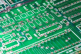
Insertion PCB assembly, a fundamental process in the electronics manufacturing industry, involves the placement and soldering of components onto a printed circuit board (PCB). This method, often referred to as through-hole technology, contrasts with surface mount technology (SMT), where components are mounted directly onto the surface of the PCB. Understanding the basics of insertion PCB assembly is crucial for those involved in electronics design and manufacturing, as it plays a significant role in determining the reliability and performance of electronic devices.
At the core of insertion PCB assembly is the use of through-hole components, which have leads that are inserted into pre-drilled holes on the PCB.
These leads are then soldered to pads on the opposite side of the board, creating a strong mechanical bond. This method is particularly advantageous for components that require a robust connection, such as connectors, transformers, and large capacitors, which are subject to mechanical stress. Moreover, through-hole technology is preferred in applications where high reliability is essential, such as in aerospace and military electronics, due to its superior mechanical strength compared to SMT.
The insertion process begins with the design and fabrication of the PCB, which includes drilling holes at precise locations to accommodate the component leads.
Once the PCB is prepared, the assembly process can commence. Components are typically inserted manually or with the aid of automated insertion machines, depending on the complexity and volume of the production run. Manual insertion is often used for small-scale production or for components that are difficult to automate, while automated insertion is preferred for high-volume manufacturing due to its speed and accuracy.
Following the insertion of components, the next critical step is soldering.
Wave soldering is the most common method used in insertion PCB assembly. In this process, the assembled PCB is passed over a wave of molten solder, which flows into the holes and around the leads, forming a secure electrical and mechanical connection. This method is efficient for soldering a large number of through-hole components simultaneously and ensures consistent solder joints. However, for prototypes or small batches, hand soldering may be employed, allowing for greater flexibility and control over the soldering process.
Quality control is an integral part of insertion PCB assembly, ensuring that the final product meets the required specifications and standards.
Inspections are conducted at various stages of the assembly process, including visual inspections to check for correct component placement and solder joint quality. Additionally, electrical testing is performed to verify the functionality of the assembled PCB, identifying any defects that may have occurred during assembly.
In conclusion, insertion PCB assembly remains a vital technique in the electronics manufacturing industry, offering distinct advantages in terms of mechanical strength and reliability. While surface mount technology has gained popularity due to its ability to accommodate smaller and more complex components, through-hole technology continues to be indispensable for specific applications. Understanding the intricacies of insertion PCB assembly, from component insertion to soldering and quality control, is essential for producing high-quality electronic devices that meet the demands of various industries. As technology continues to evolve, the integration of both through-hole and surface mount technologies will likely become more prevalent, allowing manufacturers to leverage the strengths of each method to optimize their production processes.
Key Benefits Of Insertion PCB Assembly In Modern Electronics
Insertion PCB assembly, often referred to as through-hole technology, remains a pivotal process in the manufacturing of modern electronics. Despite the rise of surface-mount technology (SMT), insertion PCB assembly continues to offer distinct advantages that make it indispensable in certain applications. Understanding these benefits is crucial for electronics manufacturers aiming to optimize their production processes and product performance.
One of the primary advantages of insertion PCB assembly is its superior mechanical strength.
Components in through-hole technology are inserted into pre-drilled holes on the PCB and soldered on the opposite side, creating a robust physical bond. This makes them particularly suitable for applications where the device may be subject to mechanical stress or vibration. For instance, in automotive and aerospace industries, where reliability under harsh conditions is paramount, through-hole components are often preferred due to their enhanced durability.
Moreover, insertion PCB assembly facilitates easier manual adjustments and repairs.
Unlike SMT, where components are mounted directly onto the surface of the PCB, through-hole components can be easily removed and replaced if necessary. This is particularly beneficial during the prototyping phase or in low-volume production runs, where design changes are frequent. The ability to quickly swap out components without damaging the PCB can significantly reduce development time and costs.
In addition to mechanical strength and ease of repair, insertion PCB assembly offers improved thermal performance
.The leads of through-hole components extend through the PCB, allowing for better heat dissipation compared to surface-mounted components. This characteristic is especially advantageous in high-power applications where efficient thermal management is critical to prevent overheating and ensure long-term reliability. Consequently, power supplies and amplifiers often utilize through-hole components to leverage this thermal advantage.
Furthermore, insertion PCB assembly provides a higher level of reliability in terms of electrical connectivity.
The solder joints in through-hole technology are generally more robust than those in SMT, reducing the risk of connection failures over time. This reliability is crucial in mission-critical applications, such as medical devices and industrial equipment, where component failure can have severe consequences. By ensuring a stable and long-lasting connection, through-hole technology helps maintain the integrity and functionality of these essential devices.
While the benefits of insertion PCB assembly are clear, it is important to acknowledge that this technology is not without its limitations.
The process is typically more labor-intensive and time-consuming than SMT, which can lead to higher production costs. Additionally, the need for drilled holes can limit the density of components on the PCB, potentially resulting in larger and heavier devices. However, for applications where the advantages of mechanical strength, repairability, thermal performance, and reliability outweigh these drawbacks, insertion PCB assembly remains a valuable choice.
In conclusion, insertion PCB assembly continues to play a vital role in the electronics manufacturing landscape. Its unique benefits make it an ideal choice for applications requiring enhanced durability, ease of repair, superior thermal management, and reliable electrical connections. As technology continues to evolve, the strategic use of through-hole technology alongside surface-mount techniques will enable manufacturers to produce high-quality, reliable electronic devices that meet the diverse needs of modern consumers and industries.
Common Challenges And Solutions In Insertion PCB Assembly
Insertion PCB assembly, a critical process in the manufacturing of electronic devices, involves placing components onto a printed circuit board (PCB) through pre-drilled holes. This method, also known as through-hole technology, is favored for its durability and reliability, especially in applications where mechanical stress is a concern. However, despite its advantages, insertion PCB assembly presents several challenges that manufacturers must address to ensure optimal performance and efficiency.
One of the primary challenges in insertion PCB assembly is the alignment of components.
Ensuring that each component is accurately placed into its corresponding hole is crucial for the functionality of the final product. Misalignment can lead to poor electrical connections, which may result in device failure. To mitigate this issue, manufacturers often employ automated insertion machines equipped with advanced vision systems. These systems enhance precision by using cameras and sensors to guide the placement of components, thereby reducing the likelihood of human error.
Another significant challenge is soldering, which is essential for securing components to the PCB and establishing electrical connections.
Insertion PCB assembly typically uses wave soldering, where the board passes over a wave of molten solder. However, this process can lead to defects such as solder bridges, where excess solder creates unintended connections between adjacent pins. To address this, manufacturers can optimize the soldering parameters, such as temperature and conveyor speed, to ensure a consistent and controlled application of solder. Additionally, implementing thorough inspection protocols, including automated optical inspection (AOI), can help identify and rectify soldering defects early in the production process.
Component variability also poses a challenge in insertion PCB assembly.
Components from different suppliers may have slight variations in size or lead configuration, which can affect their fit and function on the PCB. To overcome this, manufacturers can establish stringent quality control measures and work closely with suppliers to ensure component consistency. Furthermore, designing PCBs with some degree of tolerance can accommodate minor variations, thus enhancing the assembly process’s robustness.
Thermal management is another critical aspect that can impact the reliability of insertion PCB assemblies.
Components generate heat during operation, and inadequate heat dissipation can lead to overheating and potential failure. To address this, manufacturers can incorporate heat sinks, thermal vias, and other cooling mechanisms into the PCB design. Additionally, selecting materials with high thermal conductivity for the PCB substrate can further improve heat dissipation.
Finally, the complexity of modern electronic devices often necessitates the integration of both through-hole and surface-mount components on a single PCB. This hybrid approach can complicate the assembly process, as it requires different handling and soldering techniques for each component type. To streamline production, manufacturers can adopt a sequential assembly process, where surface-mount components are placed and soldered first, followed by the insertion of through-hole components. This approach minimizes handling and reduces the risk of damage to delicate surface-mount components.
In conclusion, while insertion PCB assembly presents several challenges, manufacturers can employ a combination of advanced technologies, meticulous process optimization, and strategic design considerations to overcome these obstacles. By addressing issues such as component alignment, soldering defects, component variability, thermal management, and hybrid assembly, manufacturers can enhance the reliability and performance of their electronic products, ultimately meeting the demands of an increasingly complex and competitive market.

Future Trends In Insertion PCB Assembly Technology
Insertion PCB assembly, a cornerstone of electronic manufacturing, is undergoing significant transformations driven by technological advancements and market demands. As we look to the future, several trends are poised to redefine this critical process, enhancing efficiency, precision, and adaptability in the production of electronic devices.
To begin with, automation is increasingly becoming integral to insertion PCB assembly.
The adoption of automated insertion machines is accelerating, driven by the need for higher throughput and reduced labor costs. These machines are equipped with advanced sensors and software that allow for precise component placement, minimizing errors and improving overall product quality. As technology continues to evolve, we can expect these machines to become even more sophisticated, incorporating artificial intelligence to further enhance their capabilities. This will enable manufacturers to handle more complex assemblies with greater ease and accuracy.
In addition to automation, the trend towards miniaturization is also influencing insertion PCB assembly.
As electronic devices become smaller and more compact, the components used in these devices must also shrink. This presents a challenge for traditional insertion methods, which are often designed for larger components. However, advancements in micro-insertion technology are addressing this issue, allowing for the precise placement of tiny components on densely packed PCBs. This trend is likely to continue as consumer demand for smaller, more powerful devices grows.
Moreover, the rise of the Internet of Things (IoT) is having a profound impact on insertion PCB assembly.
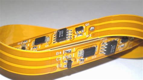
IoT devices require highly reliable and efficient PCBs to function effectively, and this is driving innovation in assembly techniques. Manufacturers are increasingly adopting flexible PCBs, which offer greater versatility and can be used in a wider range of applications. This shift is prompting the development of new insertion methods that can accommodate the unique requirements of flexible PCBs, such as their need for greater durability and resistance to environmental factors.
Sustainability is another key trend shaping the future of insertion PCB assembly.
As environmental concerns become more pressing, manufacturers are seeking ways to reduce waste and energy consumption in their production processes. This has led to the exploration of eco-friendly materials and the implementation of more efficient manufacturing techniques. For instance, the use of lead-free solder and recyclable materials is becoming more common, reflecting a broader industry commitment to sustainability. Additionally, energy-efficient machines and processes are being developed to minimize the carbon footprint of PCB assembly.
Furthermore, the integration of digital technologies is revolutionizing insertion PCB assembly.
The use of digital twins, for example, allows manufacturers to create virtual models of their assembly lines, enabling them to optimize processes and identify potential issues before they occur. This not only improves efficiency but also reduces the likelihood of costly errors and rework. Similarly, the implementation of Industry 4.0 principles, such as the use of data analytics and machine learning, is enhancing decision-making and process control in PCB assembly.
In conclusion, the future of insertion PCB assembly is being shaped by a confluence of technological advancements and evolving market demands. Automation, miniaturization, IoT, sustainability, and digital integration are all playing pivotal roles in driving innovation and improving the efficiency and effectiveness of this essential manufacturing process. As these trends continue to develop, they will undoubtedly lead to even more sophisticated and adaptable assembly techniques, ensuring that the industry remains at the forefront of technological progress.