Flex pcb vias
Understanding The Role Of Vias In Flex PCB Design
In the realm of modern electronics, the design and functionality of printed circuit boards (PCBs) are pivotal to the performance and reliability of electronic devices. Among the various types of PCBs, flexible PCBs, or flex PCBs, have gained significant attention due to their ability to bend and conform to complex shapes, making them ideal for compact and dynamic applications.
A critical component in the design of flex PCBs is the via, which plays an essential role in establishing electrical connections between different layers of the circuit. Understanding the role of vias in flex PCB design is crucial for engineers and designers aiming to optimize the performance and durability of their electronic products.
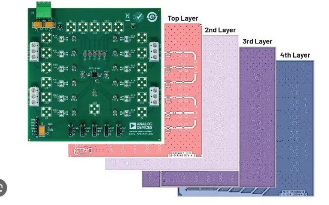
Vias are small holes drilled into the PCB that allow for electrical connections between the various layers of the board.
In flex PCBs, these vias are particularly important due to the unique challenges posed by the flexible nature of the substrate material. Unlike rigid PCBs, flex PCBs must maintain their electrical integrity while being subjected to bending, twisting, and other mechanical stresses. Therefore, the design and placement of vias in flex PCBs require careful consideration to ensure that they do not become points of failure under mechanical stress.
One of the primary considerations in the design of vias for flex PCBs is the choice of via type.
There are several types of vias, including through-hole vias, blind vias, and buried vias, each with its own advantages and limitations. Through-hole vias are the most common and extend through the entire thickness of the PCB, providing robust connections but potentially adding unnecessary weight and rigidity. Blind vias, on the other hand, connect an outer layer to one or more inner layers without passing through the entire board, offering a more space-efficient solution. Buried vias are located entirely within the inner layers, invisible from the outer surfaces, and are used to maximize surface area for component placement.
In addition to selecting the appropriate via type, designers must also consider the size and placement of vias in flex PCBs.
The size of the via is determined by the current-carrying requirements and the available space on the board. Smaller vias are often preferred in flex PCBs to maintain flexibility, but they must be large enough to handle the required current without overheating. Placement is equally critical; vias should be strategically located to minimize stress concentration and avoid areas that experience significant bending. This careful placement helps prevent mechanical failure and ensures the longevity of the PCB.
Moreover, the material used for via plating is another important factor.
Typically, vias are plated with copper to ensure good electrical conductivity. However, in flex PCBs, additional considerations such as the ductility and adhesion of the plating material are crucial. The plating must be able to withstand repeated flexing without cracking or delaminating, which could lead to circuit failure.
In conclusion, vias are indispensable components in the design of flex PCBs, serving as vital conduits for electrical connections across multiple layers. The choice of via type, size, placement, and plating material all play significant roles in ensuring the reliability and performance of flex PCBs. As electronic devices continue to evolve, demanding more compact and flexible solutions, the importance of understanding and optimizing via design in flex PCBs becomes increasingly paramount. By addressing these considerations, designers can create robust and efficient flex PCBs that meet the rigorous demands of modern electronic applications.
Best Practices For Designing Vias In Flexible PCBs
When designing flexible printed circuit boards (PCBs), one of the critical considerations is the implementation of vias, which are essential for establishing electrical connections between different layers of the board.
Vias in flexible PCBs present unique challenges and opportunities compared to their rigid counterparts, necessitating a careful approach to ensure reliability and performance. Understanding the best practices for designing vias in flexible PCBs is crucial for engineers and designers aiming to optimize their designs for both functionality and durability.
To begin with, it is important to recognize the inherent differences between flexible and rigid PCBs.
Flexible PCBs are designed to bend and twist, which means that the vias must be able to withstand mechanical stress without compromising electrical integrity. Therefore, selecting the appropriate via type is a fundamental step in the design process. Typically, there are three main types of vias used in flexible PCBs: through-hole vias, blind vias, and buried vias. Each type has its own advantages and limitations, and the choice largely depends on the specific application and design requirements.
Through-hole vias are the most common type and are often used in flexible PCBs due to their simplicity and robustness.
However, they can be more susceptible to mechanical stress, especially in areas of the board that experience frequent bending. To mitigate this, it is advisable to place through-hole vias in regions of the PCB that are less likely to flex. Additionally, reinforcing the vias with additional plating can enhance their durability.
Blind and buried vias, on the other hand, offer a more compact solution, as they do not pass through the entire board.
This can be particularly advantageous in high-density designs where space is at a premium. However, these vias require more complex manufacturing processes and can be more expensive. Therefore, their use should be carefully justified by the design’s specific needs.
Another critical aspect of via design in flexible PCBs is the consideration of via size and spacing.
Smaller vias can save space and allow for more compact designs, but they also pose a higher risk of failure due to increased current density and potential for mechanical stress. Therefore, it is essential to balance the need for miniaturization with the reliability of the vias. Ensuring adequate spacing between vias is also crucial to prevent electrical interference and potential short circuits.
Furthermore, the choice of materials plays a significant role in the performance of vias in flexible PCBs.
The materials used for the dielectric layers and the conductive plating must be compatible with the flexing nature of the board. Polyimide is a popular choice for the substrate due to its excellent flexibility and thermal stability. For the conductive layers, using materials with high ductility, such as rolled annealed copper, can help prevent cracking and ensure long-term reliability.
In addition to material selection, the manufacturing process itself must be carefully controlled to ensure the quality of the vias.
This includes precise drilling and plating techniques to avoid defects that could compromise the board’s performance. Regular testing and inspection during the manufacturing process can help identify potential issues early and ensure that the final product meets the required specifications.
In conclusion, designing vias in flexible PCBs requires a comprehensive understanding of the unique challenges posed by the flexible nature of these boards. By carefully selecting via types, optimizing size and spacing, choosing appropriate materials, and maintaining stringent manufacturing standards, designers can create flexible PCBs that are both reliable and efficient. These best practices not only enhance the performance of the final product but also contribute to its longevity, making them essential considerations in the design process.
Common Challenges And Solutions For Flex PCB Vias
Flex PCB vias, integral components in flexible printed circuit boards, present unique challenges that require careful consideration and innovative solutions. As the demand for smaller, more efficient electronic devices grows, the role of flex PCBs becomes increasingly significant. These flexible circuits allow for compact, lightweight designs, but the incorporation of vias—small holes that allow electrical connections between different layers of the PCB—introduces complexities that must be addressed to ensure optimal performance and reliability.
One of the primary challenges associated with flex PCB vias is maintaining mechanical integrity.
Unlike rigid PCBs, flex circuits are subject to bending and flexing, which can place stress on the vias. This stress can lead to cracking or delamination, potentially causing circuit failure. To mitigate this risk, designers often employ techniques such as staggered via placement, which distributes stress more evenly across the board. Additionally, using teardrop-shaped pads around vias can help reduce stress concentration, thereby enhancing the mechanical robustness of the circuit.
Another significant challenge is ensuring reliable electrical performance.
The small size and high density of vias in flex PCBs can lead to issues such as increased resistance and potential signal integrity problems. To address these concerns, it is crucial to optimize the via design. This can involve selecting the appropriate via type, such as microvias, which are smaller and can be more easily integrated into high-density designs. Furthermore, employing advanced plating techniques, such as copper filling, can improve conductivity and reduce the risk of voids or other defects that could compromise electrical performance.
Thermal management is also a critical consideration when dealing with flex PCB vias.
The compact nature of these circuits can lead to heat buildup, which can adversely affect both the vias and the overall performance of the PCB. To combat this, designers can incorporate thermal vias, which help dissipate heat by providing a path for it to escape from the board. Additionally, using materials with high thermal conductivity and designing the layout to facilitate heat dissipation can further enhance thermal management.
Manufacturing flex PCBs with vias presents its own set of challenges.
The flexible nature of the substrate can complicate the drilling and plating processes required to create vias. To overcome these difficulties, manufacturers often employ specialized equipment and techniques tailored to the unique properties of flex materials. For instance, laser drilling is commonly used for creating precise, clean via holes in flexible substrates. Moreover, ensuring proper adhesion of the plating material is crucial, as poor adhesion can lead to via failure. This can be achieved through careful surface preparation and the use of advanced plating chemistries.
In conclusion, while flex PCB vias present several challenges, a combination of thoughtful design, advanced materials, and specialized manufacturing techniques can effectively address these issues. By understanding the unique demands of flex circuits and implementing appropriate solutions, designers and manufacturers can ensure that flex PCBs meet the rigorous performance and reliability standards required in today’s electronic devices. As technology continues to evolve, ongoing research and development in this field will undoubtedly lead to even more innovative solutions, further enhancing the capabilities of flex PCBs and expanding their applications across various industries.
Innovations In Via Technology For Flexible Circuit Boards
In recent years, the electronics industry has witnessed significant advancements in the design and manufacturing of flexible circuit boards, commonly known as flex PCBs. These innovations have been driven by the increasing demand for smaller, lighter, and more versatile electronic devices.
One of the critical components that have seen substantial development in this domain is the via technology used in flex PCBs.
Vias, which are small conductive pathways that connect different layers of a circuit board, play a crucial role in ensuring the functionality and reliability of these flexible circuits. As the industry continues to push the boundaries of what is possible with flex PCBs, innovations in via technology have become a focal point for researchers and manufacturers alike.
To begin with, the traditional via technology used in rigid PCBs has been adapted and refined to meet the unique challenges posed by flexible circuits.
Unlike their rigid counterparts, flex PCBs must endure bending, twisting, and other mechanical stresses without compromising their electrical performance. Consequently, the vias in these circuits must be designed to maintain their integrity under such conditions. One of the key innovations in this area is the development of microvias, which are significantly smaller than conventional vias. These microvias not only save space but also enhance the flexibility of the circuit by reducing the amount of material that needs to be displaced during bending.
Moreover, the introduction of laser-drilled vias has revolutionized the manufacturing process of flex PCBs.
Laser drilling allows for the creation of highly precise and consistent vias, which is essential for maintaining the reliability of the circuit. This technology has enabled manufacturers to produce vias with diameters as small as 50 micrometers, thereby facilitating the design of more compact and intricate circuits. Additionally, laser-drilled vias can be created with a higher aspect ratio, meaning they can be deeper relative to their diameter. This capability is particularly beneficial for multilayer flex PCBs, where vias must traverse multiple layers to establish the necessary electrical connections.
In addition to these advancements, the use of advanced materials has also contributed to the evolution of via technology in flex PCBs.
Conductive adhesives and inks, for instance, have been developed to replace traditional metal plating in some applications. These materials offer several advantages, including improved flexibility, reduced weight, and enhanced resistance to environmental factors such as moisture and temperature fluctuations. By leveraging these materials, manufacturers can produce flex PCBs that are not only more durable but also more adaptable to a wide range of applications.
Furthermore, the integration of via-in-pad technology has emerged as a promising solution for optimizing the layout of flex PCBs.
This approach involves placing vias directly within the pads of surface-mounted components, thereby minimizing the space required for routing traces. As a result, designers can achieve higher component densities and more efficient use of the available board area. This innovation is particularly valuable in applications where space is at a premium, such as in wearable devices and medical implants.
In conclusion, the ongoing innovations in via technology for flexible circuit boards are paving the way for the next generation of electronic devices. By addressing the unique challenges associated with flex PCBs, these advancements are enabling the creation of circuits that are not only more compact and reliable but also more versatile and adaptable to a wide range of applications. As the demand for flexible electronics continues to grow, it is likely that we will see even more exciting developments in this field, further expanding the possibilities for what can be achieved with flex PCBs.

