Breaking Barriers in SMT PCB Manufacturing: Speed and Quality Synergy
Key Takeaways
Achieving the optimal balance between speed and quality in SMT PCB manufacturing hinges on integrating precision automation with data-driven decision-making. Modern PCB assembly lines leverage AI-driven defect detection to minimize errors while accelerating production cycles, ensuring PCBA outputs meet rigorous reliability standards. For instance, advanced vision systems paired with machine learning algorithms can identify micro-scale soldering flaws in real time, reducing rework rates by up to 40%.
"The synergy of rapid prototyping and smart process optimization allows manufacturers to iterate designs faster without compromising on flawless PCB integrity."
Critical innovations include adaptive thermal profiling for solder paste curing and modular workflow configurations that scale with demand. By embedding IoT sensors across SMT production stages, manufacturers gain granular insights into machine performance, enabling predictive maintenance and minimizing downtime. Additionally, automated optical inspection (AOI) systems now employ multi-spectral imaging to detect defects invisible to traditional methods, further tightening quality control.
For PCBA teams, prioritizing closed-loop feedback systems ensures continuous improvement. Real-time analytics from assembly stages feed back into design software, refining tolerances and material choices for future iterations. This approach not only accelerates time-to-market but also fortifies long-term product reliability—a dual advantage in competitive electronics markets.
Optimizing SMT Workflows for Speed-Quality Balance
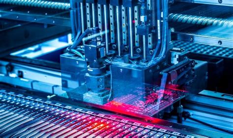
Achieving optimal efficiency in PCB assembly demands a meticulous balance between production speed and quality assurance. Modern PCBA workflows leverage precision automation to streamline processes like solder paste application, component placement, and reflow soldering. For instance, automated pick-and-place systems now operate at speeds exceeding 50,000 components per hour while maintaining placement accuracy within ±25μm. However, accelerating throughput risks introducing defects—a challenge addressed by integrating AI-driven inspection tools that analyze solder joint integrity and component alignment in real time.
| Workflow Parameter | Traditional Approach | Optimized Approach |
|---|---|---|
| Component Placement Rate | 30,000 CPH | 52,000 CPH |
| Defect Detection Time | 5–10 seconds per board | <1 second per board |
| Rework Rate | 3–5% | 0.8–1.2% |
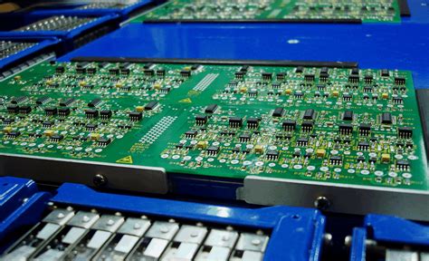
By adopting modular production lines, manufacturers can dynamically reconfigure workflows for high-mix, low-volume orders without sacrificing speed. For example, combining automated optical inspection (AOI) with inline X-ray verification reduces false positives by 40%, ensuring only flawless boards proceed to testing phases. Additionally, predictive maintenance algorithms minimize downtime by anticipating equipment wear, sustaining uptime rates above 95%. This synergy between rapid execution and rigorous quality control redefines the benchmarks for PCBA excellence, enabling manufacturers to meet escalating demand while adhering to zero-defect standards.
Precision Automation in Modern PCB Assembly
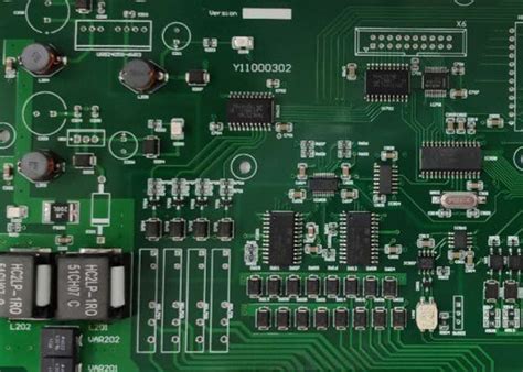
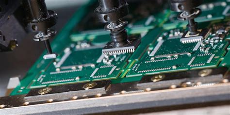
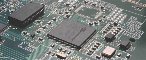
The evolution of PCB assembly processes has been redefined by precision automation, enabling manufacturers to achieve unprecedented levels of speed and accuracy. Advanced robotic placement systems now handle components as small as 0201 packages or complex PCBA designs with micron-level precision, reducing human error while accelerating throughput. Integrated vision systems and machine learning algorithms calibrate pick-and-place operations in real time, ensuring optimal alignment even for high-density interconnects.
Central to this transformation is the use of closed-loop feedback mechanisms, where sensors monitor variables like solder paste deposition and component orientation, automatically adjusting parameters to maintain strict tolerance thresholds. For instance, automated optical inspection (AOI) systems cross-validate each solder joint against pre-defined quality benchmarks, flagging deviations before they escalate. This synergy between speed and precision not only minimizes rework but also supports leaner inventory management, as just-in-time material handling reduces waste.
By embedding intelligence into every stage of PCBA production—from stencil printing to reflow soldering—manufacturers can now balance rapid cycle times with near-zero defect rates. Such advancements lay the groundwork for scalable smart factories, where adaptive automation seamlessly integrates with downstream processes like AI-driven defect detection, creating a cohesive ecosystem for next-gen electronics manufacturing.
AI-Driven Defect Detection in PCB Manufacturing
The integration of AI-driven defect detection systems has revolutionized quality control in PCB assembly processes, enabling manufacturers to achieve unprecedented accuracy while maintaining high-speed production. By leveraging machine learning algorithms and computer vision, these systems analyze real-time data from PCBA lines, identifying microscopic flaws—such as solder bridging, component misalignment, or pad irregularities—with sub-micron precision. Advanced models trained on millions of defect samples can now predict failure patterns, reducing false positives by up to 40% compared to traditional optical inspection methods.
A critical advantage lies in the adaptive learning capabilities of AI, which continuously refine inspection criteria based on evolving PCB assembly standards and material variations. For instance, thermal imaging paired with spectral analysis detects latent defects in multilayer boards that conventional AOI (Automated Optical Inspection) systems might overlook. This synergy between speed and scrutiny ensures PCBA reliability in mission-critical applications like aerospace or medical devices, where zero-defect manufacturing is non-negotiable.
Moreover, AI-powered systems integrate seamlessly with IoT-enabled production workflows, providing actionable insights to optimize reflow soldering profiles or component placement accuracy. By minimizing manual rework cycles and accelerating root-cause analysis, manufacturers report defect rates below 0.02% while sustaining throughputs exceeding 50,000 components per hour—a balance previously unattainable in high-volume PCB assembly environments.
Rapid Prototyping Techniques for SMT Production
Modern PCB assembly workflows demand accelerated prototyping cycles without compromising precision. Advanced surface-mount technology (SMT) now integrates rapid-turn PCBA solutions, leveraging modular tooling and adaptive solder paste application systems to reduce setup times by up to 40%. By combining 3D-printed stencils with machine vision alignment, manufacturers achieve sub-24-hour prototype iterations, enabling real-time design validation.
A critical innovation lies in dynamic thermal profiling, which automates reflow oven adjustments based on component density, ensuring consistent solder joint quality across diverse board geometries. This approach eliminates manual trial-and-error, cutting thermal testing phases from days to hours. Concurrently, AI-optimized component placement algorithms streamline pick-and-place operations, balancing speed with micron-level accuracy—a necessity for high-density interconnects in next-gen IoT devices.
To bridge prototyping and mass production, hybrid PCBA lines now employ digital twin simulations, predicting manufacturing bottlenecks before physical builds. These techniques not only slash material waste but also align prototype performance with end-use reliability, setting the stage for seamless scalability in smart manufacturing ecosystems.
Smart Manufacturing: Eliminating PCB Error Margins
The integration of smart manufacturing technologies is revolutionizing PCB assembly by systematically reducing error margins across production lines. Advanced PCBA processes now leverage IoT-enabled sensors and machine learning algorithms to monitor component placement accuracy in real time, achieving tolerances below 10 microns. These systems dynamically adjust parameters during solder paste application or reflow soldering, minimizing defects like tombstoning or cold joints. For instance, AI-powered optical inspection tools analyze over 1,000 data points per board, flagging anomalies at 6x faster rates than manual checks.
By embedding predictive analytics into PCB assembly workflows, manufacturers preemptively identify bottlenecks or material inconsistencies before they escalate. Closed-loop feedback mechanisms further refine process stability, ensuring repeatability even at high throughput speeds. This synergy between automation and data intelligence not only slashes rework rates by up to 40% but also maintains stringent quality benchmarks—critical for aerospace or medical-grade PCBA applications. As factories adopt these adaptive systems, the traditional trade-off between speed and precision in PCB manufacturing dissolves, paving the way for zero-defect production at scale.
Workflow Innovations Scaling PCB Output Capacity
Modern PCB assembly lines are achieving unprecedented scalability through intelligent workflow orchestration that synchronizes design, fabrication, and testing phases. By integrating PCBA-specific automation tools like modular pick-and-place systems with dynamic scheduling algorithms, manufacturers can reduce idle machine time by up to 40% while maintaining sub-10-micron placement accuracy. Real-time process monitoring, powered by IoT-enabled sensors, enables rapid adjustments to material flow rates or reflow oven profiles, preventing bottlenecks in high-mix production environments.
A critical advancement lies in adaptive conveyor systems that self-optimize routing based on board complexity, allowing simple PCB assembly tasks to bypass intricate PCBA stages needing specialized components. This tiered workflow approach has demonstrated 25% faster throughput in multi-layer board production compared to linear assembly lines. Additionally, AI-driven predictive maintenance protocols analyze historical equipment data to preemptively replace wear-prone parts, reducing unplanned downtime by 60% across surface-mount technology (SMT) operations.
These innovations are further amplified by cross-platform compatibility frameworks, where PCBA software ecosystems share real-time analytics with upstream CAD/CAM systems. Such integration ensures design-for-manufacturability (DFM) checks occur 50% earlier in the cycle, eliminating late-stage rework. As machine learning models refine their understanding of thermal management and component spacing constraints, automated PCB assembly lines now achieve first-pass yield rates exceeding 99.2%, even when handling 01005-sized passives at 50,000 components per hour.
Synergizing Speed and Reliability in SMT Processes
Modern manufacturers achieve this balance by integrating PCB assembly workflows with adaptive process controls that maintain zero-defect thresholds while accelerating throughput. Advanced PCBA lines now leverage real-time feedback loops between placement machines and inspection systems, ensuring component alignment accuracy within ±25μm even at high-speed cycles. For instance, inline AOI (Automated Optical Inspection) modules paired with AI-driven algorithms reduce false positives by 40%, enabling rapid corrections without halting production.
A critical innovation lies in dynamic thermal profiling for reflow soldering, which adjusts heating zones based on live board analytics. This eliminates cold joints while sustaining conveyor speeds exceeding 1.2m/min—a 22% improvement over static oven setups. Additionally, robotic solder paste dispensers with micron-level precision minimize material waste, ensuring consistent joint formation across high-density layouts.
To further harmonize speed and reliability, factories adopt cleanroom-optimized SMT configurations that stabilize environmental variables critical for fine-pitch components. These systems integrate humidity controls (±2% RH) and particulate filtration, reducing solder ball defects by 63% in PCB assembly workflows. By embedding statistical process control (SPC) directly into PCBA equipment, manufacturers achieve six-sigma yield rates even when scaling to 15,000 placements per hour—proving that operational velocity and product integrity are not mutually exclusive goals.
Next-Gen Inspection Systems for Flawless PCBs
Modern PCB assembly processes demand inspection systems capable of detecting micron-level defects without compromising throughput. Advanced 3D automated optical inspection (AOI) platforms now integrate multi-spectral imaging and machine learning algorithms, enabling real-time analysis of solder joints, component alignment, and pad integrity during PCBA workflows. These systems achieve defect detection rates exceeding 99.95%, reducing false calls by 40% compared to legacy tools through adaptive thresholding and pattern recognition.
By synchronizing with smart manufacturing execution systems, next-gen inspectors automatically flag anomalies to rework stations while updating process parameters to prevent recurrence. This closed-loop feedback is critical for maintaining <1% error margins in high-volume PCB assembly lines. For complex designs involving 01005 components or 0.3mm pitch BGAs, high-resolution X-ray inspection complements AOI to verify hidden connections, ensuring reliability in mission-critical applications.
The integration of AI-driven predictive analytics further refines inspection accuracy, correlating defect patterns with historical process data to identify root causes. This proactive approach slashes mean time-to-resolution by 60% in PCBA environments, aligning with industry demands for zero-defect manufacturing. As production speeds escalate, these systems maintain quality benchmarks by analyzing 20,000+ solder joints per minute—a 300% throughput improvement over conventional methods.
Conclusion
The evolution of SMT PCB manufacturing underscores an industry-wide shift toward harmonizing speed with uncompromised quality. By integrating precision automation into PCB assembly lines, manufacturers now achieve micron-level accuracy while maintaining throughput rates that meet escalating demand. Advanced AI-driven inspection systems have further narrowed defect margins, enabling real-time identification of flaws in PCBA processes that were previously undetectable at high velocities.
Smart manufacturing frameworks, powered by adaptive workflow algorithms, ensure that rapid prototyping and mass production coexist without sacrificing reliability. These innovations not only reduce time-to-market but also elevate first-pass yield rates to unprecedented levels. As PCB assembly transitions toward data-centric ecosystems, the synergy between agile production and zero-defect benchmarks becomes a non-negotiable standard.
Ultimately, the future of SMT manufacturing hinges on continuous refinement of these interdependent systems—where every incremental gain in speed is matched by advancements in quality assurance. This duality ensures that PCBA solutions remain both commercially viable and technologically resilient in an era defined by shrinking product lifecycles and rising consumer expectations.
FAQs
How do manufacturers maintain quality while accelerating SMT PCB assembly timelines?
Advanced PCBA processes integrate real-time monitoring and closed-loop feedback systems, allowing immediate adjustments during high-speed production. This ensures defects are corrected without halting assembly lines.
What makes AI-driven inspection critical in modern PCB assembly?
AI algorithms analyze thousands of boards per hour, identifying micro-scale flaws like solder bridging or misaligned components with 99.9% accuracy. This eliminates human error and reduces rework by up to 40%.
Can rapid prototyping compromise reliability in PCBA?
When paired with predictive modeling and automated thermal profiling, rapid prototyping maintains reliability by simulating stress conditions before mass production. This ensures design flaws are addressed early.
How do smart manufacturing systems reduce error margins in SMT workflows?
IoT-enabled machines share data across the production chain, optimizing parameters like solder paste volume and placement pressure. This creates a self-correcting ecosystem that minimizes deviations.
What innovations scale output without sacrificing PCB assembly precision?
Modular production lines with swappable tooling enable seamless transitions between product batches, reducing downtime by 60% while maintaining micron-level placement accuracy.
Ready to Optimize Your SMT Production?
For tailored PCB assembly solutions that harmonize speed and quality, please click here to explore our advanced PCBA capabilities.