The Impact of PCB Characteristics on Power Distribution Network (PDN) Performance
Abstract
This paper examines how various printed circuit board (PCB) characteristics significantly influence Power Distribution Network (PDN) performance in modern electronic systems. As power delivery requirements become more stringent with decreasing supply voltages and increasing current demands, understanding PCB-related factors affecting PDN impedance, noise, and stability becomes crucial. The analysis covers dielectric materials, stackup design, via configurations, plane layers, and layout considerations that collectively determine PDN effectiveness. Practical design recommendations are provided to optimize PDN performance through careful PCB engineering.
1. Introduction
The Power Distribution Network (PDN) serves as the critical infrastructure that delivers stable and clean power to all active components on a PCB. With modern ICs operating at lower voltages (often below 1V) while drawing higher currents (exceeding 100A in some processors), the PDN must maintain voltage regulation within tight tolerances despite rapidly changing dynamic loads. The PCB itself plays a fundamental role in PDN performance, acting as both the physical medium for power delivery and a significant contributor to overall impedance and noise characteristics.
This paper explores how specific PCB attributes influence key PDN metrics including target impedance, transient response, ripple voltage, and resonance effects. By understanding these relationships, designers can make informed decisions during PCB development to ensure robust power delivery.
2. PCB Dielectric Materials and PDN Performance
2.1 Dielectric Constant (Dk) and Loss Tangent
The choice of PCB dielectric material directly affects power plane capacitance and high-frequency performance. Materials with higher dielectric constants (Dk) provide greater interplane capacitance according to the relationship:
C = ε₀εᵣA/d
Where ε₀ is vacuum permittivity, εᵣ is relative Dk, A is plane area, and d is separation distance. While increased capacitance benefits high-frequency decoupling, materials with higher Dk typically exhibit greater dispersion (frequency-dependent Dk variation), which complicates impedance control across broad bandwidths.
The loss tangent (tan δ) determines dielectric absorption at high frequencies. Materials with lower loss tangents (e.g., Rogers 4350B at 0.0037) minimize power dissipation in the dielectric, reducing PDN losses compared to standard FR-4 (tan δ ≈ 0.02).
2.2 Material Thickness and Layer Stackup
Dielectric thickness between power and ground planes establishes both plane capacitance and characteristic impedance. Thinner dielectrics increase capacitance but reduce impedance, which can exacerbate transmission line effects. A typical balance for moderate-speed designs uses 2-4 mil dielectrics between adjacent power/ground pairs.
Modern high-performance designs often employ hybrid stackups combining different dielectric materials—using low-Dk, low-loss materials for high-speed signal layers and higher-Dk materials for power integrity optimization.
3. Power Plane Design Considerations
3.1 Plane Shapes and Splits
The geometry of power planes significantly impacts current distribution and PDN impedance. Solid planes offer lowest impedance but become impractical in multi-rail designs. When splits become necessary:
- Avoid creating narrow neck regions that increase local impedance
- Maintain adequate spacing between different voltage domains (typically 20-50 mil)
- Consider the current return paths for signals crossing plane splits
3.2 Plane Proximity and Coupling
Adjacent power planes exhibit mutual capacitance that can either benefit or degrade PDN performance. Closely spaced planes (2-3 mil) provide natural high-frequency decoupling but may introduce unwanted coupling between voltage domains. Strategic placement of ground planes between different power rails reduces crosstalk while maintaining decoupling benefits.
4. Via Effects on PDN Impedance
4.1 Via Inductance
Every via connection in the PDN contributes parasitic inductance according to:
L ≈ μ₀h/2π [ln(4h/d) + 1]
Where h is via length and d is via diameter. This inductance creates impedance spikes that degrade high-frequency performance. Mitigation strategies include:
- Using multiple vias in parallel (reduces effective inductance)
- Minimizing via length through optimized layer stackup
- Employing via-in-pad techniques for critical components
4.2 Via Stubs
Unused via portions below connection points act as stubs that introduce resonant discontinuities. Back-drilling (controlled-depth drilling) removes these stubs in high-frequency designs to maintain PDN impedance control.
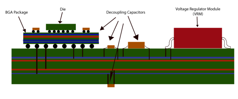
5. Decoupling Capacitor Implementation
5.1 Mounting Inductance
The effectiveness of decoupling capacitors depends largely on PCB-related mounting inductance:
L_mount ≈ L_via + L_trace + L_ESL
Where L_via is via inductance, L_trace is connecting trace inductance, and L_ESL is capacitor equivalent series inductance. To minimize this:
- Place capacitors as close as possible to power pins
- Use short, wide connection traces
- Implement symmetric via arrangements (multiple vias per pad)
5.2 Plane Spreading Inductance
Even with ideal capacitor mounting, current must spread through planes to reach devices. The spreading inductance depends on plane separation:
L_spread ≈ μ₀d/π ln(D/d)
Where d is dielectric thickness and D is distance to device. This explains why thin dielectrics benefit high-frequency decoupling.
6. PCB Layout Techniques for PDN Optimization
6.1 Component Placement Strategy
Strategic placement of power-hungry components relative to voltage regulators reduces PDN impedance:
- Distribute high-current devices evenly across the board
- Locate sensitive analog circuits away from digital switching hotspots
- Implement localized power islands for critical subsystems
6.2 Current Density Management
Analyzing current density distribution helps identify potential PDN bottlenecks:
- Widen traces or use copper pours for high-current paths
- Avoid right-angle turns in power traces (increases local inductance)
- Use thermal reliefs judiciously—they increase impedance
7. Advanced PCB Technologies for PDN Enhancement
7.1 Embedded Capacitance Materials
Thin (0.5-2 mil) dielectric layers with high Dk (20-50) laminated between power/ground planes provide distributed decoupling capacitance. These materials effectively reduce high-frequency impedance without discrete capacitors.
7.2 Buried Power Rails
Some high-density designs incorporate dedicated power routing layers with thicker copper (2-4 oz) to minimize DC resistance. These layers often use low-Dk dielectrics to prevent excessive capacitance.
7.3 3D Power Delivery
Advanced packaging techniques like silicon interposers enable three-dimensional power distribution, reducing traditional PCB PDN limitations. However, this shifts rather than eliminates PCB design challenges.
8. Measurement and Verification Techniques
8.1 Frequency Domain Analysis
Vector network analyzer (VNA) measurements of PDN impedance validate design choices:
- Measure from DC to GHz frequencies
- Compare results with target impedance profiles
- Identify resonant peaks for mitigation
8.2 Time Domain Analysis
Oscilloscope measurements capture transient response to load steps:
- Verify voltage droop meets specifications
- Correlate time-domain events with frequency-domain characteristics
- Evaluate effectiveness of decoupling networks
9. Conclusion
PCB characteristics profoundly influence PDN performance through multiple interacting mechanisms. Optimal PDN design requires co-optimization of dielectric materials, stackup architecture, via configurations, plane geometries, and component placement. As power requirements continue evolving, PCB technologies must advance to support lower impedances at higher frequencies while managing cost and manufacturability constraints. By systematically addressing each PCB parameter affecting PDN behavior, designers can achieve robust power delivery in even the most demanding electronic systems.