Understanding Board-Level Decoupling in PCB Design
Introduction to Decoupling in Electronics
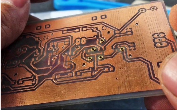
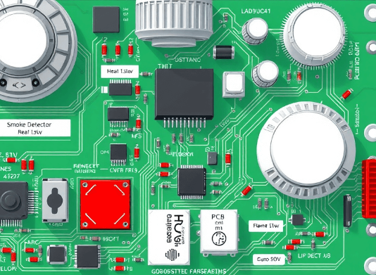
In modern printed circuit board (PCB) design, managing power distribution has become increasingly critical as electronic devices continue to shrink in size while growing in complexity and performance. One of the most essential techniques for ensuring stable power delivery is decoupling, particularly at the board level. Board-level decoupling refers to the strategic placement of capacitors across a PCB to maintain power integrity by reducing noise, suppressing voltage fluctuations, and preventing unwanted interactions between different circuit components.
The importance of proper board-level decoupling cannot be overstated. In high-speed digital systems, fast-switching integrated circuits (ICs) can create sudden current demands that the main power supply cannot immediately satisfy due to inherent inductance in the power distribution network (PDN). Without adequate decoupling, these transient current demands can cause voltage droops (sags) or spikes that may lead to signal integrity issues, timing errors, or even complete system failures.
The Physics Behind Power Distribution Challenges
To fully appreciate the need for board-level decoupling, we must examine the fundamental electrical characteristics of power distribution systems. Every conductor in a PCB, including power and ground planes, possesses three inherent properties: resistance (R), inductance (L), and capacitance (C). While resistance causes DC voltage drops, inductance presents the primary challenge for high-frequency operation.
The relationship between voltage (V), inductance (L), and current change over time (di/dt) is given by:
V = L × (di/dt)
When a digital IC switches states, it can create extremely rapid current changes (high di/dt). Even small inductances in the power delivery path can result in significant voltage fluctuations. For example, a 100mA current change in 1ns through just 10nH of inductance produces a 1V spike—potentially devastating for modern ICs operating at 1.8V or lower.
Decoupling Capacitor Fundamentals
Decoupling capacitors serve as local energy reservoirs that can supply transient currents much faster than the main power supply. When placed close to power-hungry components, these capacitors:
- Provide immediate charge for fast current transients
- Reduce the effective inductance seen by the IC
- Filter high-frequency noise
- Create a low-impedance path between power and ground
The effectiveness of a decoupling capacitor depends on several factors:
- Capacitance value: Determines how much charge can be stored
- Equivalent series resistance (ESR): Affects how quickly energy can be delivered
- Equivalent series inductance (ESL): Limits high-frequency performance
- Physical size: Impacts parasitic properties and placement options
- Dielectric material: Influences frequency response and temperature stability

Multi-Tiered Decoupling Approach
Effective board-level decoupling typically employs a hierarchical approach using capacitors of different values and characteristics:
Bulk Decoupling (10-100μF)
These larger capacitors, usually electrolytic or tantalum, serve as the first line of defense. They handle lower frequency fluctuations (typically below 1MHz) and replenish the charge of smaller capacitors. Placed near power entry points or voltage regulators, bulk capacitors compensate for slower response times of the main power supply.
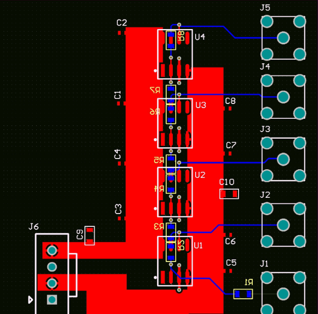
Board-Level Decoupling (0.1-10μF)
Medium-value ceramic capacitors (often 0.1μF or 1μF) distributed across the PCB form the backbone of the decoupling strategy. These address mid-frequency noise (1MHz to 100MHz) and are typically placed at regular intervals in the power distribution network, especially near groups of ICs.
Local/Component-Level Decoupling (1nF-0.1μF)
Small ceramic capacitors placed as close as possible to individual IC power pins combat high-frequency noise (above 100MHz). Their proximity is crucial because parasitic inductance increases with connection length, reducing effectiveness at higher frequencies.
PCB Layout Considerations for Optimal Decoupling
Proper physical implementation is just as important as capacitor selection. Key layout guidelines include:
- Minimizing loop area: Place decoupling capacitors close to IC power pins with short, wide traces to reduce inductance.
- Via placement: Use multiple vias for connections to power and ground planes to lower impedance.
- Power plane capacitance: Leverage the inherent capacitance between closely spaced power and ground planes.
- Capacitor orientation: Align capacitors to minimize current path length to ICs.
- Layer transitions: Optimize the path from capacitor to IC through different layers.
A common mistake is focusing solely on the nominal capacitance value while neglecting the actual impedance profile. Due to parasitic inductance and resistance, each capacitor has a self-resonant frequency where it’s most effective. Above this frequency, the capacitor becomes inductive and less effective.
Frequency Domain Analysis of Decoupling Networks
The impedance of an ideal capacitor decreases with frequency (Z = 1/(2πfC)). However, real capacitors exhibit a V-shaped impedance curve due to parasitic elements:
- At low frequencies: Impedance dominated by capacitance (decreasing with frequency)
- At resonant frequency: Minimum impedance determined by ESR
- At high frequencies: Impedance dominated by ESL (increasing with frequency)
This behavior necessitates using multiple capacitor values in parallel to create a low-impedance profile across a broad frequency spectrum. When properly implemented, the parallel combination yields a lower and flatter impedance curve than any single capacitor could achieve alone.
Advanced Decoupling Techniques
As digital systems push into the multi-gigahertz range, traditional decoupling approaches face new challenges:
Embedded Capacitance
Some high-performance PCBs incorporate thin dielectric materials between power and ground planes to create distributed capacitance across the entire board. This “plane capacitance” provides excellent high-frequency decoupling with minimal inductance.
Interdigitated Capacitors
These specialized structures combine multiple capacitor elements in interlocking patterns to reduce overall ESL while maintaining high capacitance density.
Dielectric Materials
Advanced materials with high permittivity (high-k) allow for greater capacitance in smaller form factors, though often with tradeoffs in voltage rating or temperature stability.
3D Packaging
Technologies like package-on-package (PoP) and system-in-package (SiP) integrate decoupling capacitors within the IC package itself, minimizing interconnect inductance.
Simulation and Measurement of Decoupling Performance
Modern PCB design relies heavily on simulation tools to predict and optimize decoupling performance:
- Power Integrity Simulation: Models the impedance of the entire PDN from DC to high frequencies
- SPICE Analysis: Simulates transient response to current steps
- S-Parameter Measurements: Characterizes real-world PDN performance
Measurement techniques include:
- Vector network analyzer (VNA) for impedance measurements
- Oscilloscope with high-bandwidth probes for transient analysis
- Frequency-domain reflectometry for characterizing distributed structures
Common Decoupling Pitfalls and How to Avoid Them
Even experienced designers can fall into these traps:
- Over-reliance on a single capacitor value: Using only 0.1μF capacitors leaves gaps in frequency coverage.
- Neglecting capacitor placement: A perfectly selected capacitor placed too far from the IC becomes ineffective.
- Ignoring return current paths: Decoupling requires complete loops—poor ground connections undermine effectiveness.
- Underestimating parasitics: Tiny amounts of inductance or resistance can dominate at high frequencies.
- Overlooking temperature effects: Capacitor performance degrades at temperature extremes.
Future Trends in Board-Level Decoupling
Emerging technologies are reshaping decoupling strategies:
- Higher frequencies: 5G and millimeter-wave applications demand decoupling effective at 10s of GHz
- Smaller form factors: IoT devices require innovative decoupling in ultra-compact designs
- Wide-bandgap semiconductors: GaN and SiC devices switch faster, creating steeper di/dt challenges
- Machine learning optimization: AI-assisted PDN design and capacitor selection
- Advanced materials: Nanocomposite dielectrics and ultra-low ESL capacitor structures
Conclusion
Board-level decoupling represents a critical aspect of modern PCB design that bridges the gap between power supply capabilities and integrated circuit requirements. By understanding the underlying principles, implementing a multi-tiered capacitor strategy, and paying careful attention to layout details, designers can create robust power distribution networks that support reliable operation of even the most demanding electronic systems.
As technology continues to advance, the importance of effective decoupling only grows more pronounced. What remains constant is the fundamental goal: to provide clean, stable power to every active component on the board, regardless of its current demands or operating frequency. Mastering board-level decoupling techniques remains an essential skill for any serious PCB designer working in today’s high-speed digital landscape.