Precision and Efficiency: CNC Engraving for PCB Fabrication
Introduction
Printed Circuit Boards (PCBs) are the backbone of modern electronics, providing the necessary electrical connections between components. As electronic devices become more compact and complex, the demand for precise and efficient PCB manufacturing techniques has grown significantly. Among the various methods available, Computer Numerical Control (CNC) engraving machines have emerged as a powerful tool for PCB prototyping and small-scale production.
This article explores the process of CNC engraving for PCBs, discussing its advantages, limitations, key parameters, and best practices to achieve optimal results.
1. Understanding CNC Engraving for PCBs
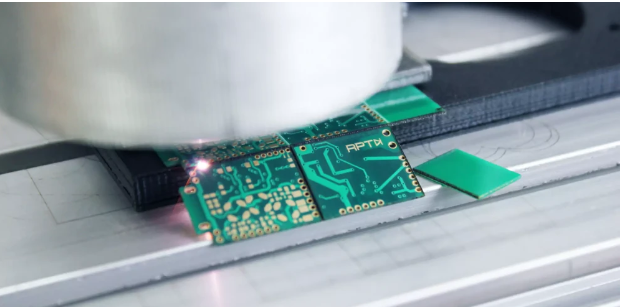
1.1 What is CNC Engraving?
CNC engraving is a subtractive manufacturing process where a computer-controlled machine uses rotating cutting tools to remove material from a substrate. In PCB fabrication, this technique is used to:
- Isolate copper traces by removing unwanted copper from the board.
- Drill holes for through-hole components and vias.
- Cut the PCB outline to the desired shape.
1.2 How Does It Work?
The process involves:
- Design Preparation: A PCB design is created using CAD software (e.g., KiCad, Eagle, Altium) and exported as Gerber files or G-code.
- Machine Setup: The CNC machine is configured with the appropriate tool (e.g., V-bit engraver, end mill) and spindle speed.
- Material Fixturing: The copper-clad board is secured onto the machine bed.
- Engraving Execution: The CNC machine follows the programmed toolpath to carve out traces and drill holes.
- Post-Processing: The board is cleaned, inspected, and, if necessary, further processed (e.g., solder mask application).
2. Advantages of CNC Engraving for PCBs
2.1 Rapid Prototyping
- Unlike traditional etching (which requires chemicals and masks), CNC engraving produces PCBs in minutes, making it ideal for quick iterations.
2.2 No Chemical Processing
- Eliminates the need for hazardous chemicals (ferric chloride, ammonium persulfate), reducing environmental impact and safety risks.
2.3 High Precision
- Modern CNC machines can achieve trace widths as fine as 0.1 mm, suitable for most hobbyist and professional applications.
2.4 Flexibility in Design Changes
- Modifications can be made directly in the CAD file without requiring new masks or stencils.
2.5 Single-Board Production
- Unlike industrial PCB fabrication (which requires panelization), CNC engraving is cost-effective for one-off boards.
3. Limitations and Challenges
3.1 Material Constraints
- CNC engraving works best on FR4 fiberglass and other rigid substrates but struggles with flexible PCBs.
3.2 Tool Wear
- Small-diameter bits wear out quickly, especially when machining abrasive materials like fiberglass.
3.3 Limited Fine-Pitch Accuracy
- While suitable for most designs, extremely dense circuits (e.g., BGA components) may require laser or photochemical methods.
3.4 Surface Roughness
- Mechanical cutting can leave burrs, requiring additional sanding or deburring.
4. Key Parameters for Optimal PCB Engraving
4.1 Tool Selection
- V-Bit Engravers (30°-60°) – Ideal for fine traces.
- End Mills (0.2-1.0 mm diameter) – Used for isolation routing and outline cutting.
- Drill Bits (0.3-3.0 mm) – For hole drilling.
4.2 Spindle Speed and Feed Rate
- Spindle Speed: 10,000–24,000 RPM (higher speeds reduce tool deflection).
- Feed Rate: 100–300 mm/min (adjust based on material and tool sharpness).
4.3 Depth of Cut
- Copper Layer: 0.05–0.1 mm (just enough to remove copper without damaging the substrate).
- Drilling Depth: Slightly deeper than the board thickness to ensure clean through-holes.
4.4 Stepover and Toolpath Strategy
- Stepover (10-30%) – Ensures complete copper removal without excessive tool wear.
- Isolation Milling – Preferred over raster engraving for better edge quality.
5. Step-by-Step PCB Engraving Process
5.1 Design Export
- Generate Gerber files or G-code from PCB design software.
- Use CAM software (e.g., FlatCAM, Carbide Create) to convert Gerber files to machine instructions.
5.2 Machine Calibration
- Zero the Z-axis precisely to avoid incomplete copper removal or excessive cutting.
- Secure the PCB firmly to prevent vibrations.
5.3 Running the Job
- Start with a test run on a scrap board to verify settings.
- Monitor the first few minutes to ensure proper tool engagement.
5.4 Post-Processing
- Remove dust and debris with compressed air or a brush.
- Inspect for broken traces or incomplete cuts.
- Apply solder mask (optional) using UV-curable ink.
6. Comparing CNC Engraving with Other PCB Methods
| Method | Pros | Cons |
|---|---|---|
| CNC Engraving | Fast, no chemicals, flexible | Limited fine-pitch, tool wear |
| Chemical Etching | High precision, low cost | Hazardous chemicals, slow |
| Laser Engraving | Extremely fine traces | Expensive, limited to thin PCBs |
| Industrial PCB Fab | Best for mass production | High cost for prototypes |
7. Future Trends in PCB Engraving
- Hybrid Machines: Combining CNC and laser engraving for finer details.
- Automated Tool Changers: Reducing manual intervention in multi-step jobs.
- AI-Based Optimization: Smart CAM software that adjusts parameters dynamically.
Conclusion
CNC engraving is a versatile and efficient method for PCB prototyping, offering speed, precision, and environmental benefits over traditional etching. While it has limitations in ultra-fine-pitch applications, advancements in machine technology continue to expand its capabilities. By optimizing tool selection, feed rates, and machining strategies, engineers and hobbyists can produce high-quality PCBs with minimal waste and maximum efficiency.
For makers, startups, and educational institutions, CNC-based PCB fabrication remains an indispensable tool in the electronics development cycle. As the technology evolves, it will likely play an even greater role in rapid prototyping and low-volume production.