How to Achieve High-performance PCB Design Engineering
Main text:
Driven by Moore’s Law,the electronics industry is seeing increasingly powerful products,higher levels of integration,faster signal speeds,and shorter product development cycles.
Consequently,PCB design has entered the era of high-speed PCB design.PCB are no longer simply a means of interconnection,but have become a crucial component in all electronic products.This article comprehensively analyzes all aspects of high-performance pcb design in the IT industry from the perspective of engineering implementation.Achieving high-performance PCB design first requires a highly qualified PCB design team.
1.Recommendations for Forming a PCB Design Team
Since PCB design entered the high-speed era,the practice of hardware engineers solely responsible for schematic and pcb design has become a thing of the past.Dedicate PCB engineers have emerged.
A mature large or medium-sized PCB design team should include the following roles:
Package library Engineer:This dedicated library engineer is familiar with the process capabilities and technical specifications of today’s mainstream board and SMT manufactures.Based on the company’s product experience ,they complete the PCB package library constuction work under current high-speed and high-density conditions.
PCB design Engineers:Designers must possess extensive knowledge of PCBs,including basic electronic circuitry,pcb production and SMT fabrication,and design for forecasting(DFX)(Design Factorization/Design for forecasting/Design for Forecasting).They also need to master high-speed pcb stackup design,impendance design,signal integrity,and EMC,They must comprehensively consider the various requirement of modem PCB design and complete PCB layout and routing.
SI Engineers:Uncover the “hidden schematics”hidden within PCB transmission lines,directly addressing reflection,crosstalk,and timing issues in the high-speed era.Through forward and backward simulations,they ensure signal quality,improve product first-time success rates,and ensure stable and reliable PCB operation.
EMC Engineer:As the source of EMC design,they are responsible for board-level EMC design,including circuits,component,and PCBs.They minimize external radiation and improve resistance to external inference.
Thermal Design Engineer:Thermal Design Engineer are indispensable in R&D teams striving for exquisite and compact products.They analyze heat source distribution and design appropriate air duct systems to control system temperature rise and ensure stable and reliable and stable products without the involvement of a thermal design engineer.(Note:Some companies have structural engineers also handle pcb thermal simulation and thermal design)
Process Engineers: Develop process parameters for the company’s PCB design based on the process capabilities of the company’s PCB fabricator and SMT equipment/manufacturer. They participate in the design of specific boards and PCBs to ensure PCB manufacturability and processability.
To ensure internal communication, technical advancement, and backup, each of the above roles should have at least three people. For companies with limited team size and fluctuating R&D needs, it’s wise to appropriately reserve a number of versatile and multifaceted individuals and seek external resources as needed to address internal R&D shortcomings.
Let’s take a look at the history of PCB design team formation at IT giants:
In 1980, in-house hardware engineers began concurrently designing PCBs.
In 1990, CAD engineers gradually became independent as a specialized department.
In 1995, professional PCB design houses became popular in North America and Japan.
In 2000, specialized work became increasingly specialized, with database construction, PCB design, SI, EMC, thermal design, and process engineering becoming increasingly independent. Over 50% of PCB design in North America and Japan is now performed by specialized design firms. SI, EMC, and other areas gradually became independent systems.
In 2003, professional design firms, led by YiBo Technology, introduced the concept of PCB design outsourcing to China.
In 2008, internal divisions of labor became clear, and the scope of work became comprehensive. The rational use of resource outsourcing, staggered design, and technology outsourcing became a trend.
II. Essential Hardware Foundation for High-Performance PCB Design
Since PCB design entered the high-speed era, signal integrity knowledge based on transmission line theory has overshadowed hardware fundamentals. Some have suggested that in ten years, hardware design will consist of only front-end and back-end components (front-end refers to IC design, back-end refers to PCB design). A systems engineer will simply be needed to integrate these components. This easily calls into question the necessity of learning hardware fundamentals. In reality, both IC and PCB engineers must possess knowledge of circuits such as R, L, C, and basic gate circuits.
High-performance PCB design requires basic knowledge of power supplies and FPGAs. Even signal integrity analysis based on transmission line theory begins with the study of infinitesimal elements based on R, L, and C.
PCB design engineers must possess fundamental circuit knowledge, such as high-frequency, low-frequency, digital circuits, microwaves, electromagnetic fields, and electromagnetic waves. Familiarity and understanding of the basic functions of the product being designed and the fundamental hardware knowledge are essential for completing high-performance PCB designs.
III. Challenges and Engineering Implementation of High-Performance PCB Design
PCB design is an art form where there is no perfect solution, only better solutions. Achieving high-performance PCB design often faces the following challenges:
1.Challenges of the R&D Cycle
Statistics show that the typical time from project initiation to market for a laptop is only six months. The average development time for a mobile phone, from project initiation to market launch, is only three months. As a crucial component of product development, PCB design time has been increasingly compressed.
In April 1985, Toshiba engineer Tetsuya Mizoguchi designed a pocket-sized computer called the T1100, which spearheaded the rise of the computer industry. Since then, the development cycle for computer motherboards has significantly accelerated.
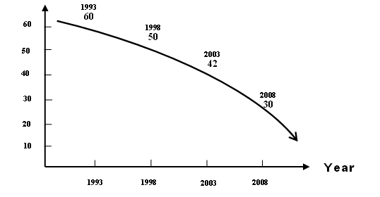
Figure 1: The Evolution of Computer Motherboard Design Cycles
At EDADOC, laptop PCB design is typically completed within three weeks, while mobile phone PCB design typically meets customer expectations of 10 days.
Faced with ever-shortening market development deadlines, how can PCB engineers meet this challenge?
First, they must adopt top-notch EDA tools.
Efficient EDA tools not only improve efficiency but also revolutionize design concepts. Among numerous EDA tools, Cadence’s PSD series undoubtedly holds a leading position in the industry. From the single-person approach of a decade ago, to the subsequent “sub-drawing” model, and now to the “partitioning” model, the multi-person concurrent design provided by Cadence Allegro has made previously impossible R&D cycles a reality. At EDADOC, 92% of PCB designs utilize concurrent design.
For example, EDADOC once completed the front-end and back-end simulation, layout, and routing of a 20,000-pin XDSL board in just six days, with concurrent design playing a significant role.
Using a typical laptop motherboard PCB design as an example, let’s examine the main PCB design data from a traditional “single-person” approach (one PCB engineer), a three-shift work model adopted by some companies, and a concurrent design approach:
Working Method: Single-person approach, three-person relay, three-shift parallel design
Design Time: 30 days, 18 days, 15 days
Advantages: Single person responsible, no handoffs, low communication costs, faster delivery, multi-person intelligence, flexible delivery schedule, easy control, multiple people working simultaneously, and easy communication. Multi-person intelligence
Disadvantages: Long turnaround time, limited knowledge base, and difficulty for engineers to accept; low efficiency during night shifts; inconvenient communication with peripheral resources; three handoffs and low transfer efficiency; requiring a relatively large team size, resulting in slightly reduced staff efficiency.
Suitable for small companies or simple single-board projects. No communication with peripheral resources is required. Complex single boards can be used in conjunction with concurrent design in exceptional cases, shortening the design cycle. Widely used in large and medium-sized EDA teams.
Secondly, early involvement in the product development process reduces subsequent rework.
PCB engineers are involved in R&D during the overall design phase, focusing on the product’s system architecture design and demonstration. During the overall design phase, they conduct initial PCB design feasibility assessments. During the detailed design phase, they collaborate with the schematic design and participate in device selection, structural design, and thermal design. This simplifies the main work once R&D enters the PCB design process, reducing rework during the PCB design process due to issues such as excessive device size, insufficient drive capability, unfeasible topology solutions, and structural heat dissipation.
Third, the “One-Board Success” design philosophy.
A senior IBM consultant once pointed out a problem facing a domestic R&D team: “There’s no time to get things done right the first time, but there’s time to do things over and over again.” In today’s competitive market, experienced PCB design engineers, a robust design process, and the use of various software tools can help achieve one-board success. This not only saves the cost of one PCB board, but also shortens the entire R&D cycle, creating a window of market opportunity for the product. Both PCB engineers and product R&D managers must embrace the “One-Board Success” philosophy in PCB R&D.
Finally, module reuse and technological accumulation.
Many well-known domestic companies I’ve worked with place great emphasis on module reuse, ensuring technological accumulation while effectively shortening PCB design time.
In short, we must proactively engage in R&D, adopt concurrent design, and embrace the “One-Board Success” philosophy to reduce R&D cycles. Combined with advanced software tools like Cadence PSD, we can address PCB R&D cycle issues without excessive overtime or double or even triple shifts.
2.Cost Challenges
PCB costs include both explicit and implicit costs.
Explicit costs primarily include PCB production and placement costs.
To control explicit costs, we can reduce them by familiarizing ourselves with the process capabilities of conventional PCB foundries and the process requirements of placement equipment, selecting an appropriate number of layers, setting a suitable stackup structure, and implementing appropriate design parameters.
Implicit costs include personnel investment, technical risks, time costs during the PCB design process, and especially the opportunity cost of the market window.
In reality, the implicit costs of PCB design far outweigh its explicit costs.
For example, the market window for a typical mobile phone is approximately six months. If additional R&D is required due to PCB design issues, for a trendy mobile phone, the result would not only be a loss of one to two months of time, but also the failure of the entire product.
To control implicit costs, company executives and R&D managers should adopt a philosophy of focusing on the core, ignoring the peripherals, combining strengths, and achieving first-time success. Costs should be considered from the outset of design. They should leverage external resources to address any shortcomings in their own R&D and reduce the implicit costs of product R&D.
3.High-Speed Challenges
With the continuous increase in signal speeds, signal integrity continues to challenge R&D personnel. This includes bus drive capability, signal reflections, crosstalk, overshoot, oscillation, backtracking, and attenuation. Timing is sometimes also considered part of signal integrity. Allegro’s IBIS-based simulation module, Signoise, facilitates topology construction and simulation.
This Allegro simulation tool interfaces well with the routing platform. After PCB routing is complete, routing parameters can be directly extracted from the PCB and imported into the Signoise platform for post-simulation verification.
The routing constraints extracted from the simulation can be directly imported into Allegro’s electrical rules manager, which facilitates the application of equal-length constraints for timing requirements. During routing, Allegro provides real-time alerts when lengths do not meet the specified rules.
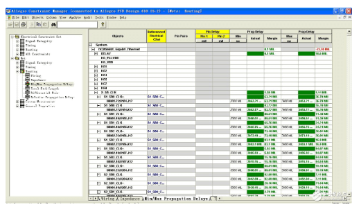
Figure 2: Rule Manager Example (Click image to enlarge)
As shown in the figure, when the length is within the specified range, the corresponding area in the table appears green. When the length is outside the specified range, whether too short or too long, the corresponding area in the table appears red.
4.The Challenge of High Density
Let’s take a look at some data:
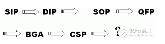
Changes in device packaging in recent years:
Changes in the number of pins per device and the total number of pins per board in the IT industry over the past 20 years:+
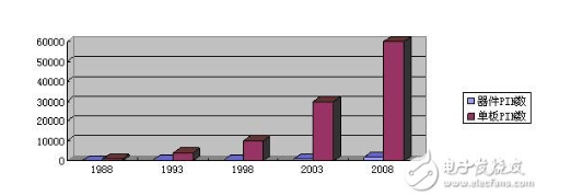
Figure 3: Changes in the number of pins per device and the total number of pins per board
Changes in the number of layers per board in the IT industry over the past 20 years:
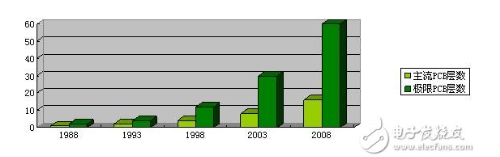
Figure 4: Changes in the number of layers per board
Changes in the number of pins per square meter per board (pins/sq in) over the past 20 years:
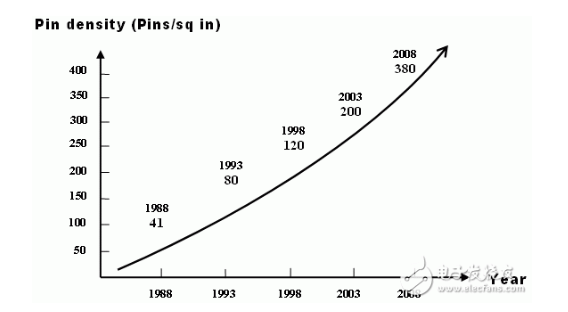
Figure 5: Changes in the number of pins per square meter per board
The above data clearly demonstrates the pressure of increasing PCB design density, from the widespread use of jumpers 20 years ago to double-sided and multi-layer boards, and then to changes in device packaging. In recent years, the rise of high-density interconnect (HDI) technology driven by the mobile phone industry, including the recent launch of Intel’s Menlow platform, has brought HDI technology to the PC industry.
Faced with the ever-increasing density of PCB designs, PCB engineers must stay abreast of industry trends, understand new materials and processes, and employ top-tier EDA software capable of supporting high-density PCB design. This is crucial to meeting the increasing density challenges faced during product development. The upcoming PSD 16.2 is said to offer significant breakthroughs in HDI design, and we look forward to it.
5.The Challenge of Power and Ground Noise
Power and ground planes serve as reference planes and return paths for signal lines. Power and ground noise can directly impact the signals using them as reference planes. Addressing power and ground noise not only requires ensuring the stability of the power supply itself but is also crucial for ensuring the reliability of high-speed signals.
Power supply design for high-speed PCBs begins with clarifying the power tree and analyzing the rationality of power supply paths.
First, when considering high-current carrying capacity, appropriate trace widths must be allocated while taking margin into account. Furthermore, due to the resistance of actual traces, voltage drops occur along the path from the power supply output to the actual load. Since the voltages of high-speed circuit components, especially the core voltage, are often very low, this voltage drop directly impacts power supply performance. Current carrying capacity is related to trace width, inner and outer layers, copper thickness, and allowable temperature rise.
Secondly, the power supply’s impedance must be considered when considering power supply filtering. This is because power channels are not ideal but rather have resistance and impedance. High-speed circuits require instantaneous power supply when gates flip. The current from the power module to each gate flip requires distribution through various paths, which takes time. This can be understood as a staged charging process.
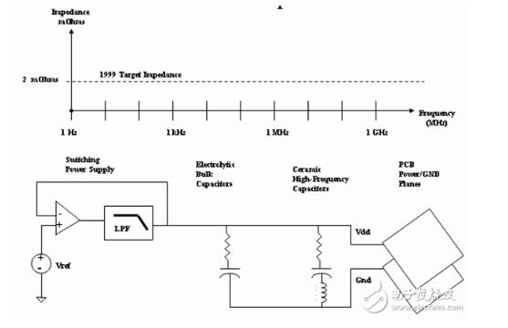
Figure 6: Gate Circuit+Flipping the Power Supply Path
As you can see, at high frequencies, the current at the device pin is first supplied by the flat plate capacitor formed by the power and ground planes, because this power supply system has the lowest impedance. This results in the fastest power supply. However, the flat plate capacitors store very little charge, so their charge is supplied by the small filter capacitors, which in turn are supplied by the large bulk capacitors. The switching power supply then charges the bulk capacitors through the current path. This is because the switching power supply has low impedance only at frequencies of a few kHz, the bulk capacitors have low impedance only at frequencies of a few MHz, and the small filter capacitors have low impedance only at frequencies of tens to hundreds of MHz. Only by charging through these layers can the current reach the device pins and meet the instantaneous power supply requirements. Cadence also provides a PI analysis module to analyze the impedance of the power planes and the appropriate selection of filter capacitors at different power consumption levels.
This PI simulation tool is based on transmission line theory. It uses finite element analysis to partition the power plane, matching the power and corresponding ground planes into a pair of flat capacitors and dividing them into several regions, as shown in the figure:
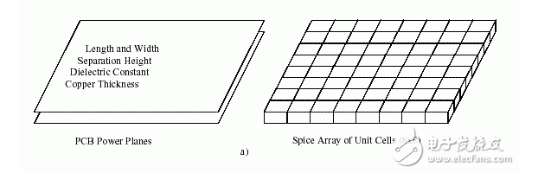
The tool uses frequency domain analysis to analyze the impedance of each small area on the board, ultimately generating an impedance plot for each point:
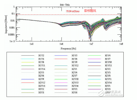
If the impedance of a point in a certain area is found to be above the target impedance, the target impedance at that point can be lowered by reallocating the power plane or adding filtering capacitors, thereby enhancing filtering capabilities for the device pins.
6.EMC Issues:
With improved living standards and increased awareness of environmental protection, including electromagnetic interference (EMC), EMC issues have become an unavoidable challenge in all electronic product development. Considered a “black magic,” EMC issues are increasingly troubling developers.
EMC must be designed from the source. As the source of product EMC, the EMC performance of boards/PCBs is gaining increasing attention. Among the many EMC indicators, the RE index is the most vexing for hardware engineers.
Due to model limitations, even the industry’s recognized top-tier EMC simulation software cannot yet produce data comparable to actual test data. It can only provide simplified radiation field distributions from a single radiating source under certain specific conditions, providing a design reference.
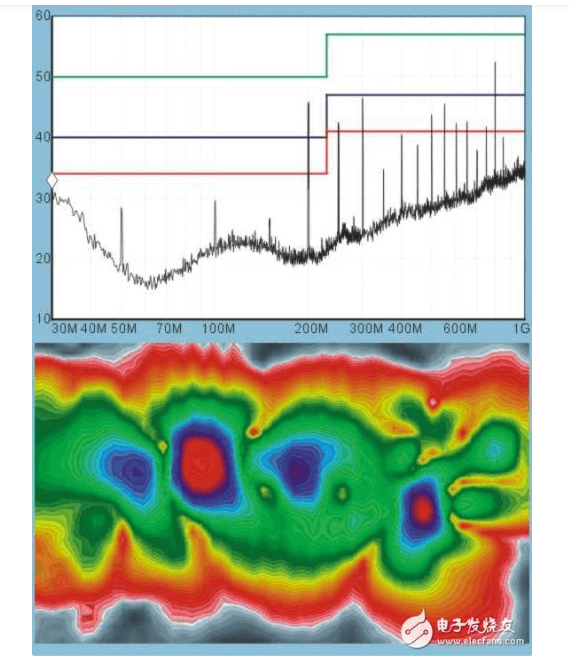
EMC design has traditionally relied primarily on the experience of EMC engineers and hardware engineers. As engineers, we don’t need extensive theoretical analysis, but we do need some general engineering experience. We also utilize auxiliary tools such as near-field probes to address EMC issues. The figure above shows the RE measured with a near-field probe and a diagram of the physical spatial distribution of EMI at specific frequencies.
In my opinion, when addressing EMC issues for single-board circuits (PCBs), we need to focus on the following three areas:
1) Power Supply
2) Clock (and other strong radiation sources)
3) Interface Circuits
When it comes to power supply, we’re considering the integrity of the power supply (ground) and the design of the power ground, which serves as the return path.
The clock is the primary source of EMI on a single board, accounting for over 60% of EMI.
Neglecting the design of any single interface can negate your entire product’s EMC efforts.
As an engineering implementation, by focusing on the three key areas above, the EMC issues for the entire product are within reach.
7.Design for Function (DFM) Challenges
To address DFM issues, in addition to having single-board process engineers develop process standards tailored to their company, PCB design engineers need to receive systematic and comprehensive DFM training. PCB engineers need to continuously monitor the industry’s PCB production and processing capabilities and, based on their company’s specific circumstances, select appropriate process routes and design parameters. Comprehensive consideration should be given to the trade-offs between electrical performance and DFM. Furthermore, dedicated library builders are essential for PCB package libraries to address design-for-manufacturing (DFM) issues at the source.
Allegro has a dedicated library build module that allows for easy design of package libraries and their pads based on device datasheets. Good package design is the foundation of DFM.
High-performance PCB design challenges sometimes present conflicting requirements. PCB design engineers must leverage their comprehensive experience to balance these challenges, find the optimal balance, and ultimately achieve engineering success.
Fourth, Sharp Tools Are Essential for Good Work
High-performance PCB design relies on advanced EDA tools. Cadence’s PSD series offers powerful capabilities for high-speed PCB design. Its front-end and back-end simulation modules ensure signal quality and improve first-time product success rates. Its use of physical and electrical rules enables intelligent implementation of technical requirements such as differential routing and equal-length control. It supports concurrent design, shortens R&D time, and supports module reuse and prioritizes technological advancement, ensuring design quality and improving efficiency.
High-performance EDA tools, combined with experienced PCB design engineers, ensure the realization of high-performance PCB designs. As a PCB design company with over 150 engineers, EDADOC is dedicated to high-speed, high-density, and high-performance PCB design. It has gradually become a leading force in promoting high-performance PCB design in China.