
PCB Aspect Ratio: Hole Diameter to Board Thickness Guidelines
Manufacturing defects in through-hole plating account for 15-20% of PCB failures in multilayer boards. The root cause often traces back to aspect ratio violations—drilling holes too small relative to board thickness. When aspect ratios exceed manufacturer capabilities, plating chemistry cannot reach hole bottoms, creating voids, cracks, and intermittent connections that fail during thermal cycling or vibration testing.
What Is PCB Aspect Ratio?
PCB aspect ratio is the ratio of total board thickness to the finished hole diameter after plating. This dimensionless value determines manufacturing feasibility for through-hole vias and component holes.
The calculation is straightforward:
Aspect Ratio = Board Thickness ÷ Finished Hole Diameter
For example, a 1.6 mm thick board with a 0.20 mm finished hole yields an 8:1 aspect ratio (1.6 ÷ 0.20 = 8). This means the drill must penetrate eight times deeper than the hole width, directly affecting plating uniformity and reliability.
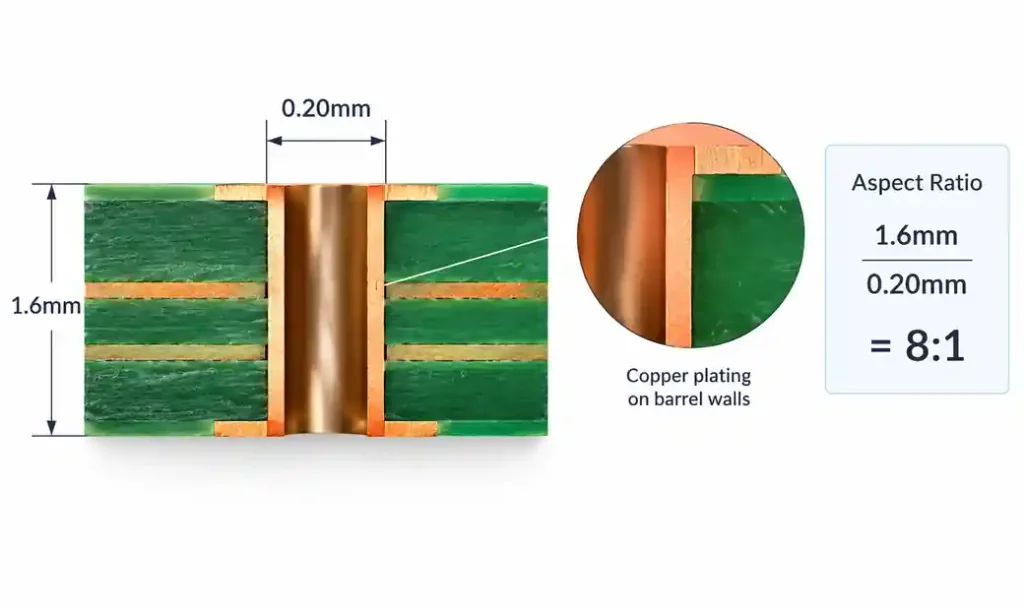
You need to consider aspect ratio during stackup design because it constrains minimum hole sizes for your chosen board thickness. A 10-layer board at 2.4 mm thickness requires larger vias than a 4-layer board at 1.0 mm to maintain the same aspect ratio.
According to IPC-6012 qualification standards, acceptable aspect ratios depend on hole class, copper weight, and reliability requirements. Standard manufacturing supports 8:1 to 10:1, while advanced facilities achieve 12:1 or higher with specialized processes.
Why Aspect Ratio Matters for PCB Manufacturing
Aspect ratio directly impacts three critical manufacturing processes: mechanical drilling, hole cleaning, and electroplating. Each process faces escalating challenges as aspect ratios increase.
During mechanical drilling, high aspect ratios generate excessive heat and friction. A 0.20 mm drill penetrating 2.4 mm depth (12:1 ratio) experiences chip evacuation problems. Debris cannot escape the narrow channel, causing drill breakage, hole wall roughness, and dimensional variations that affect final hole quality.
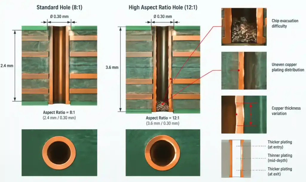
Plating chemistry struggles to deposit uniform copper in high aspect ratio holes. The electroplating solution relies on ion transport and agitation to reach deep hole walls. At 10:1 ratios, the center section receives 30-40% less copper than hole ends. At 12:1, this disparity increases to 50-60%, creating thin spots prone to cracking during thermal expansion.
For multilayer HDI designs, microvia aspect ratios follow different rules. Laser-drilled microvias typically maintain 0.75:1 to 1:1 ratios, allowing reliable plating in holes as small as 0.10 mm diameter.
Standard PCB Aspect Ratio Capabilities
PCB manufacturers classify aspect ratio capabilities into three tiers based on equipment sophistication and process control. Understanding these tiers helps you design within feasible manufacturing windows.
| Capability Level | Aspect Ratio Range | Board Thickness Example | Minimum Hole Size | Manufacturing Process |
|---|---|---|---|---|
| Standard | 6:1 to 8:1 | 1.6 mm | 0.20 mm | Conventional drilling, standard plating |
| Advanced | 8:1 to 10:1 | 2.0 mm | 0.20 mm | High-speed drilling, enhanced plating |
| Specialized | 10:1 to 12:1 | 2.4 mm | 0.20 mm | Precision drilling, specialized chemistry |
| Extreme | 12:1 to 15:1 | 3.0 mm | 0.20 mm | Sequential drilling, multiple plating cycles |
Standard 8:1 capability covers 80% of commercial electronics applications. You can design 1.6 mm boards with 0.20 mm finished holes or 2.4 mm boards with 0.30 mm holes without special processes.
Advanced 10:1 capability requires tighter process control. Manufacturers use pulse plating or modified chemistry to improve deep-hole copper distribution. Lead times increase 2-3 days, and costs rise 15-25% compared to standard ratios.
Specialized processes above 10:1 involve sequential drilling and plating. Thick boards receive partial drilling, first plating cycle, then complete drilling and final plating. This two-step approach ensures adequate copper coverage but doubles processing time and cost.
Andwin Circuits manufactures boards up to 50 layers with controlled aspect ratios, supporting both standard 8:1 processes and advanced 12:1 capabilities for thick multilayer designs requiring deep vias.
High Aspect Ratio Challenges and Solutions
High aspect ratio drilling introduces three failure modes: incomplete plating, voiding, and copper cracking. Each requires specific design countermeasures.
Incomplete Plating at Hole Centers
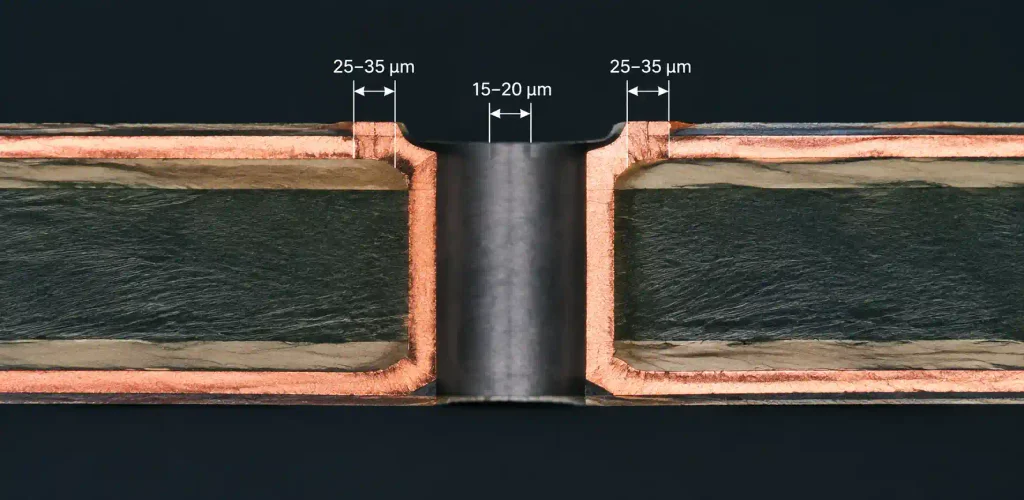
Copper thickness varies along hole depth in high aspect ratio vias. Typical plating deposits 25-35 μm at hole ends but only 15-20 μm at the center of a 12:1 hole. This 40% reduction creates weak points susceptible to current overload and thermal stress.
The solution involves specifying minimum plating thickness per IPC-6012 Class 3 requirements: 25 μm average with 20 μm minimum anywhere in the hole. Manufacturers achieve this through extended plating time, pulse plating, or additive processes that build up thinner deposits more uniformly.
Voiding and Gas Entrapment
Drilling deep narrow holes traps air pockets and residual drilling fluid. When heated during reflow, trapped gases expand and rupture thin plating, creating voids. These voids appear as open circuits or intermittent connections during electrical testing.
Prevention requires thorough hole cleaning before plating. Desmear processes using permanganate chemistry remove drilling smear and open resin-filled microcracks. Plasma cleaning provides additional assurance for holes above 10:1 ratio.
Copper Cracking During Thermal Cycling
Differential thermal expansion between copper (CTE 17 ppm/°C) and FR4 (CTE 14-16 ppm/°C in-plane, 60-80 ppm/°C z-axis) generates stress in plated holes. High aspect ratio vias with thin center plating crack first, typically within 100-500 thermal cycles between -40°C and +125°C.
Design solutions include increasing finished hole size to reduce aspect ratio, specifying high-Tg materials with lower z-axis CTE, or using filled vias that mechanically support thin plating during expansion cycles.
Calculating Optimal Aspect Ratio for Your Design
Aspect ratio optimization balances board thickness requirements, via density needs, and manufacturing cost. Follow this calculation sequence:
Step 1: Determine Required Board Thickness
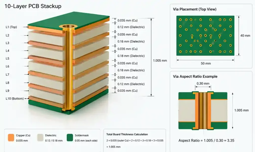
Calculate stackup thickness from layer count, copper weight, and dielectric requirements. A 10-layer board with 1 oz copper (35 μm) and standard FR4 prepreg typically reaches 1.8-2.0 mm finished thickness.
Step 2: Identify Minimum Via Size
High-density routing may require 0.20 mm or 0.25 mm finished holes. Through-hole components specify minimum hole sizes in datasheets, typically 0.70-1.20 mm for standard packages.
Step 3: Calculate Aspect Ratio
Divide board thickness by smallest required hole:
- 2.0 mm ÷ 0.20 mm = 10:1 (advanced capability needed)
- 2.0 mm ÷ 0.25 mm = 8:1 (standard capability sufficient)
Step 4: Evaluate Manufacturing Feasibility
Compare calculated ratio against manufacturer capabilities. Ratios above 10:1 require special processes, longer lead times, and higher costs. Consider design alternatives:
- Reduce board thickness by optimizing copper weight (0.5 oz inner layers instead of 1 oz)
- Increase via drill size from 0.20 mm to 0.25 mm (reduces routing density 15-20%)
- Use staggered vias or back-drilling to reduce effective depth
- Specify HDI construction with buried vias that don’t span full thickness
| Design Scenario | Board Thickness | Via Hole Size | Aspect Ratio | Recommendation |
|---|---|---|---|---|
| 4-layer standard | 1.6 mm | 0.25 mm | 6.4:1 | Optimal – standard process |
| 8-layer standard | 2.0 mm | 0.25 mm | 8:1 | Good – standard process |
| 12-layer dense | 2.4 mm | 0.20 mm | 12:1 | Challenging – advanced process needed |
| 16-layer thick | 3.2 mm | 0.25 mm | 12.8:1 | Difficult – consider HDI or back-drilling |
For automotive applications requiring AEC-Q100 qualification, limit aspect ratios to 8:1 for better thermal cycling performance. Medical devices under IPC Class 3 typically specify 10:1 maximum with 25 μm minimum plating thickness verification.
Impact of Aspect Ratio on Layer Count
Board layer count directly affects achievable aspect ratios. Each additional layer pair adds 0.20-0.30 mm thickness, progressively limiting minimum via sizes.
Layer Count vs Thickness Relationship
Standard stackup constructions follow predictable thickness patterns:
- 4-layer: 0.8-1.0 mm → supports 0.10 mm holes at 8:1 ratio
- 6-layer: 1.2-1.4 mm → supports 0.15 mm holes at 8:1 ratio
- 8-layer: 1.6-1.8 mm → supports 0.20 mm holes at 8:1 ratio
- 10-layer: 2.0-2.2 mm → supports 0.25 mm holes at 8:1 ratio
- 14-layer: 2.6-2.8 mm → supports 0.30 mm holes at 8:1 ratio
- 20-layer: 3.2-3.6 mm → supports 0.40 mm holes at 8:1 ratio
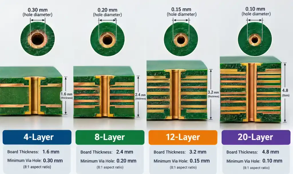
This progression explains why high layer count boards use larger vias. A 20-layer board physically cannot accommodate 0.20 mm through-holes at standard 8:1 ratios without special processes.
HDI Solutions for Thick Boards
High layer count designs exceeding 12 layers benefit from HDI construction with buried and blind vias. These structures limit via depth to 3-4 layers instead of full board thickness, maintaining favorable aspect ratios:
A 16-layer board at 3.0 mm thickness would require 0.375 mm holes for 8:1 ratio. Using 1+N+1 HDI construction, blind vias span only 0.6-0.8 mm depth, allowing 0.10 mm holes at comfortable 6-8:1 ratios.
Andwin Circuits supports up to 50-layer PCB manufacturing using advanced HDI techniques. These designs use stacked and staggered microvias combined with buried via structures to maintain aspect ratios within 8:1 to 10:1 range throughout the stackup.
Design Optimization Strategies
Five strategies help optimize aspect ratio without sacrificing board functionality or manufacturability.
Strategy 1: Selective Via Sizing
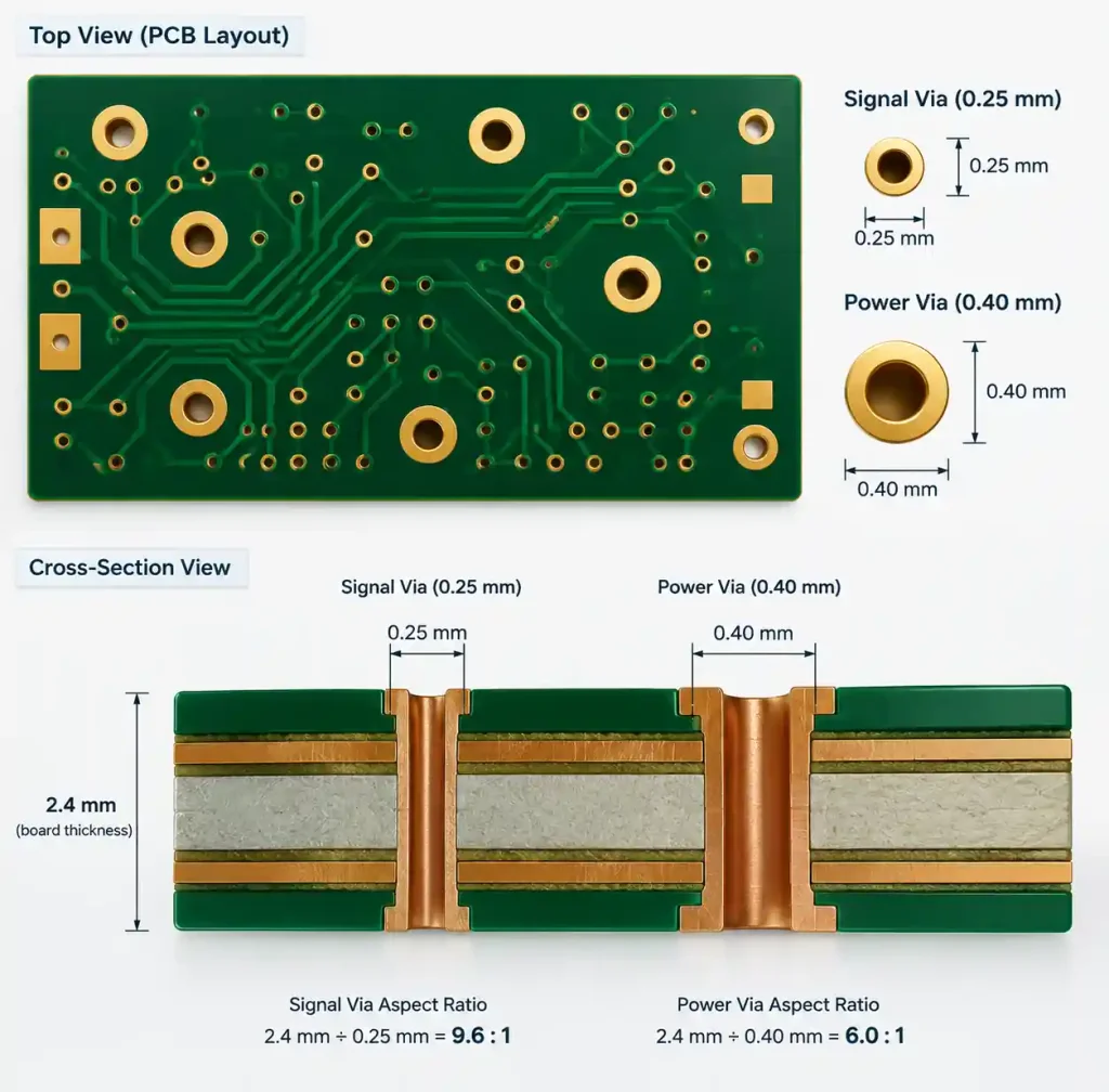
Not all vias require minimum drill size. Power and ground vias carrying high current benefit from larger holes that reduce resistance and improve thermal performance. Route signal vias at minimum size, but specify 0.30-0.40 mm for power distribution.
This mixed via approach maintains 8:1 aspect ratios on critical small vias while allowing thicker boards. A 2.4 mm thick design uses 0.25 mm signal vias (9.6:1) and 0.40 mm power vias (6:1), averaging acceptable ratios across the design.
Strategy 2: Back-Drilling for Thick Boards
Back-drilling removes unused via stubs on high-speed signals, improving signal integrity while effectively reducing aspect ratio. A through-hole via in a 3.0 mm board gets back-drilled from bottom side, removing 1.5 mm of unused barrel. The remaining 1.5 mm depth with 0.25 mm hole yields 6:1 aspect ratio instead of 12:1.
This technique proves essential for high-frequency designs above 5 GHz where via stubs create impedance discontinuities and resonances.
Strategy 3: Staggered Via Patterns
Dense routing sometimes requires closely spaced vias that create aspect ratio challenges. Staggered vias offset positions on adjacent layers, allowing buried vias that span 4-6 layers instead of full thickness.
A 12-layer board uses three groups of staggered buried vias (L1-L6, L4-L9, L7-L12) instead of through-holes. Each buried via spans 1.2 mm instead of 2.4 mm full thickness, halving the aspect ratio.
Strategy 4: Material Selection
High-Tg FR4 and polyimide materials offer lower z-axis CTE (50-60 ppm/°C) compared to standard FR4 (70-80 ppm/°C). Reduced expansion decreases stress on high aspect ratio plating, improving reliability during thermal cycling.
For boards requiring 10:1 to 12:1 ratios, specify Tg 170-180°C materials with controlled CTE. This adds 15-20% material cost but enables reliable high aspect ratio manufacturing.
Strategy 5: Sequential Build-Up
Very thick boards (>3.0 mm) benefit from sequential build-up processes. Manufacture a thin core (1.6 mm) with standard 8:1 vias, then laminate additional layer pairs with buried vias. Final assembly maintains acceptable aspect ratios throughout the structure.
This approach suits industrial control applications requiring thick copper (3-6 oz) and 16-24 layers for ruggedized power distribution.
Manufacturer Capability Verification
Before committing to production, verify manufacturer aspect ratio capabilities through three validation steps.
Review Capability Documents
Request detailed capability sheets specifying maximum aspect ratios for different board thicknesses and hole sizes. Look for specific callouts like “10:1 standard, 12:1 with qualification” rather than vague claims of “high aspect ratio capability.”
Compare your calculated worst-case ratio against stated limits. A 2.4 mm board with 0.20 mm holes (12:1) requires explicit 12:1 verification, not just “up to 12:1” marketing language.
DFM Analysis
Submit Gerber files for DFM review before quotation. Competent manufacturers flag aspect ratio violations and suggest alternatives:
- “0.20 mm holes in 2.4 mm board exceed our 10:1 standard capability”
- “Recommend increasing hole size to 0.25 mm or specify advanced process”
- “Alternative: use HDI construction with buried vias”
Missing DFM feedback on obvious aspect ratio issues indicates inadequate process control or attention to detail.
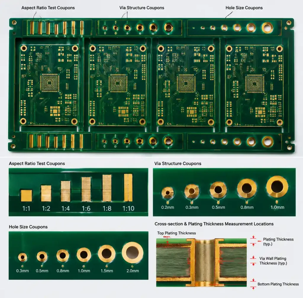
Request Test Coupons
Specify aspect ratio test coupons on your panel borders. These coupons contain representative hole sizes at your board thickness, allowing cross-section analysis of plating thickness distribution.
Acceptable plating shows <20% variation between hole ends and center. Variations exceeding 30% indicate process limits, requiring design changes or alternate manufacturers.
Andwin Circuits provides comprehensive DFM analysis and capability matching during quotation, identifying aspect ratio concerns before production commitment. Our facility certification to IATF 16949 and ISO 9001 ensures consistent process control for demanding applications.
FAQ
What is the maximum PCB aspect ratio for standard manufacturing?
Standard PCB manufacturing reliably supports 8:1 aspect ratio using conventional drilling and plating processes. This allows 1.6 mm thick boards with 0.20 mm finished holes or 2.4 mm boards with 0.30 mm holes. Advanced manufacturers achieve 10:1 with tighter process control, while specialized facilities reach 12:1 using sequential drilling and enhanced plating chemistry.
How does aspect ratio affect PCB cost?
Aspect ratios above 8:1 increase manufacturing cost by 15-30% due to slower drilling speeds, extended plating cycles, and higher scrap rates. Ratios exceeding 10:1 may require special processes like pulse plating or sequential build-up, adding 30-50% premium. Design optimization to maintain standard 8:1 ratios provides best cost-performance balance.
Can I use 0.20 mm vias in a 10-layer PCB?
Yes, if total board thickness stays below 1.6-2.0 mm. A typical 10-layer stackup ranges 2.0-2.4 mm thickness, creating 10:1 to 12:1 aspect ratios with 0.20 mm holes. This requires advanced manufacturing capability and costs 20-40% more than standard processes. Consider 0.25 mm holes to maintain 8:1 ratio for better cost and reliability.
What happens if aspect ratio is too high?
Excessive aspect ratios cause incomplete copper plating at hole centers, creating thin spots prone to cracking. Thermal cycling between -40°C and +125°C generates stress that fractures thin plating within 100-500 cycles. Electrical testing may show intermittent connections or complete opens. Design verification and manufacturer capability matching prevent these failures.
Do microvias have different aspect ratio limits?
Yes. Laser-drilled microvias in HDI designs typically maintain 0.75:1 to 1:1 aspect ratios. A 0.10 mm microvia spans only 0.10 mm depth (one layer pair), allowing reliable plating in structures too small for mechanical drilling. Stacked microvias may reach 1.5:1, but staggered arrangements maintain favorable ratios while achieving dense interconnect.
How do I calculate aspect ratio for back-drilled vias?
Use actual plated barrel length, not total board thickness. A 3.0 mm board with 0.30 mm holes creates 10:1 ratio for full through-hole. Back-drilling 1.5 mm from bottom removes half the barrel, leaving 1.5 mm plated length for 5:1 effective aspect ratio. This improves both manufacturing reliability and high-frequency signal integrity.
Conclusion
PCB aspect ratio—the relationship between board thickness and hole diameter—fundamentally determines manufacturing feasibility and reliability. Standard 8:1 ratios suit most applications, while advanced 10:1 to 12:1 capabilities require specialized processes with cost and lead time implications. Design optimization through selective via sizing, HDI construction, or back-drilling maintains favorable ratios without sacrificing functionality.
If you need multilayer PCB manufacturing with controlled aspect ratios for your electronic product, Andwin Circuits offers advanced capabilities up to 50 layers with aspect ratio optimization. Our facility is certified to ISO 9001, IATF 16949, and IPC standards, ensuring reliable plating and consistent quality. We provide comprehensive DFM analysis and fast turnaround in 7 days for prototypes.
Contact us today for custom PCB solutions, capability verification, and competitive factory-direct pricing.