
PCB for Wireless Charging: Coil Design and Qi Standard Compliance
Wireless charging failures account for 20-30% of consumer electronics returns, with improper coil design and non-compliant PCB layouts responsible for efficiency losses, overheating, and device incompatibility. When your wireless charging product must meet Qi 2.2 standards while delivering 15-25W power transfer, PCB coil design becomes critical for smartphones, wearables, and automotive applications.
What is Wireless Charging PCB?
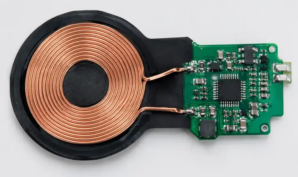
Wireless charging PCB is a printed circuit board designed with integrated or surface-mounted coils that enable inductive power transfer following Qi standards. These boards contain planar spiral copper traces forming transmitter (TX) or receiver (RX) coils operating at 100-205 kHz, replacing traditional wound litz wire coils. PCB coils achieve 85-90% efficiency while reducing thickness by 40-60% compared to wire-wound designs, making them suitable for compact devices.
The Qi 2.2 standard released in 2025 increased power delivery from 15W to 25W through Magnetic Power Profile (MPP) 2.0, which uses magnetic alignment rings for precise coil positioning. This eliminates the misalignment losses that plagued earlier wireless charging implementations.
Qi Standard Power Levels and Compliance Requirements
Qi standards define multiple power profiles for different applications. Understanding these specifications ensures your PCB design meets certification requirements.
| Power Level | Qi Profile | Typical Applications | Coil Diameter | Frequency Range | Key Requirements |
|---|---|---|---|---|---|
| 5W | Baseline Power Profile (BPP) | Budget smartphones, accessories | 40-50 mm | 110-205 kHz | Basic FOD, ±10% efficiency |
| 7.5W | BPP Extended | iPhone 8-14 series | 45-55 mm | 110-205 kHz | Enhanced thermal management |
| 10W | Extended Power Profile (EPP) | Android fast charging | 45-60 mm | 100-205 kHz | Active cooling recommended |
| 15W | EPP High Power | Premium smartphones | 50-65 mm | 87-205 kHz | Mandatory FOD per Qi 1.3 |
| 25W | MPP 2.0 (Qi 2.2) | iPhone 17, flagship devices | 55-70 mm | 360 kHz | Magnetic alignment, advanced FOD |
Compliance testing per Qi specification requires verification of power transfer efficiency (minimum 70%), foreign object detection response time (under 50ms), and electromagnetic compatibility per FCC Part 15 and CE standards.
PCB Coil Design: Planar Spiral Layout
PCB coils use planar spiral traces instead of wound wire, offering precise geometry control and automated manufacturing. Design parameters directly affect coupling coefficient, inductance, and power transfer efficiency.
Trace geometry: Circular spiral coils provide optimal coupling. Target inductance ranges from 5-15 μH for RX coils and 10-25 μH for TX coils. Use 10-20 turns with 0.3-0.8 mm trace width and 0.2-0.5 mm spacing. Wider traces reduce DC resistance but increase capacitance.
Copper weight selection: Standard 1 oz (35 μm) copper works for 5-10W applications. Use 2 oz (70 μm) copper for 15W designs to reduce I²R losses. For 25W Qi 2.2 implementations, specify 2-4 oz copper with heavy copper PCB design techniques to handle 2-3A coil currents.
Layer stackup: Single-layer coils work for RX applications. TX coils benefit from 2-layer designs where inner layers carry power traces while outer layers host the coil. Use 4-layer stackups for controlled impedance matching to 50Ω controller outputs.
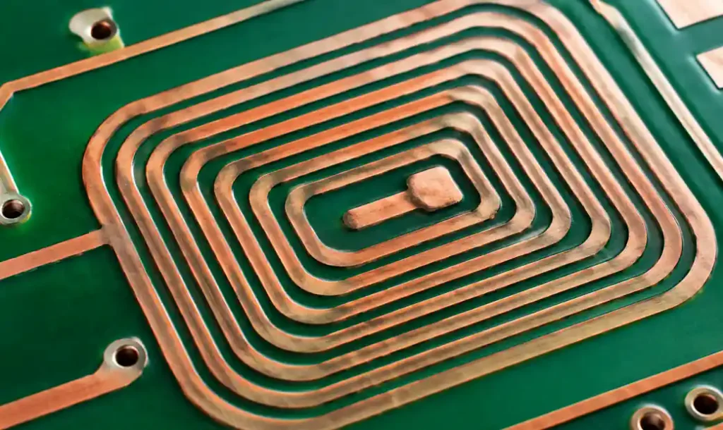
Coil spacing and clearance: Maintain 2-3 mm clearance between coil traces and other components to prevent electromagnetic interference. Space the coil center 3-5 mm from board edges to allow magnetic flux completion. For rigid flex PCB designs, position coils on rigid sections only.
Ferrite Shielding and Magnetic Field Management
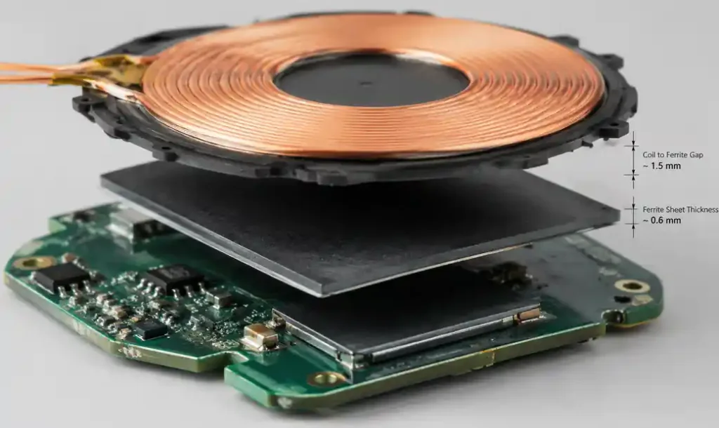
Ferrite backing is mandatory for efficient wireless charging. The ferrite sheet directs magnetic flux toward the receiving coil while shielding components behind the PCB from high-frequency fields.
Material selection: Use NiZn ferrite for frequencies above 1 MHz or MnZn ferrite for Qi’s 100-205 kHz range. Target permeability of μr = 100-300 with low coercivity (Hc < 10 A/m). Higher permeability increases inductance but risks saturation at high power levels.
Thickness optimization: RX coils require 0.1-0.3 mm ferrite sheets. TX coils need 0.3-0.5 mm thickness to prevent saturation at 15-25W power levels. Thickness beyond 0.5 mm adds minimal benefit while increasing cost and device thickness.
Coverage area: Ferrite should extend 3-5 mm beyond coil outer diameter. Full coverage prevents eddy currents in nearby metal components like battery cases or chassis. Adhesive-backed ferrite simplifies assembly and maintains consistent coil-to-ferrite distance.
Thermal Management for High-Power Wireless Charging
Qi 2.2’s 25W power transfer generates 2-4W heat dissipation in the PCB. Poor thermal design causes efficiency drops, controller shutdown, and user discomfort when charging phones exceed 40°C surface temperature.
Copper pour strategy: Add ground pours on unused PCB areas to spread heat. Connect pours to coil center tap using multiple thermal vias. A 20×20 mm copper pour with 0.5 mm via spacing reduces hotspot temperature by 8-12°C compared to isolated coils.
Thermal vias: Use arrays of 0.3 mm diameter vias spaced 0.8-1.2 mm apart beneath controller ICs and power MOSFETs. Target via density of 4-6 vias per cm². Thermal vias transfer heat to internal ground planes, leveraging the full board as a heat spreader. This technique is standard in metal core PCB designs.
Material considerations: FR-4 with Tg 170°C handles 15W charging. For 25W Qi 2.2, specify high-Tg materials (180-200°C) or polyimide for better thermal stability. PCB material properties like thermal conductivity directly affect charging speed sustainability.
Controller IC Integration and Power Stage Layout
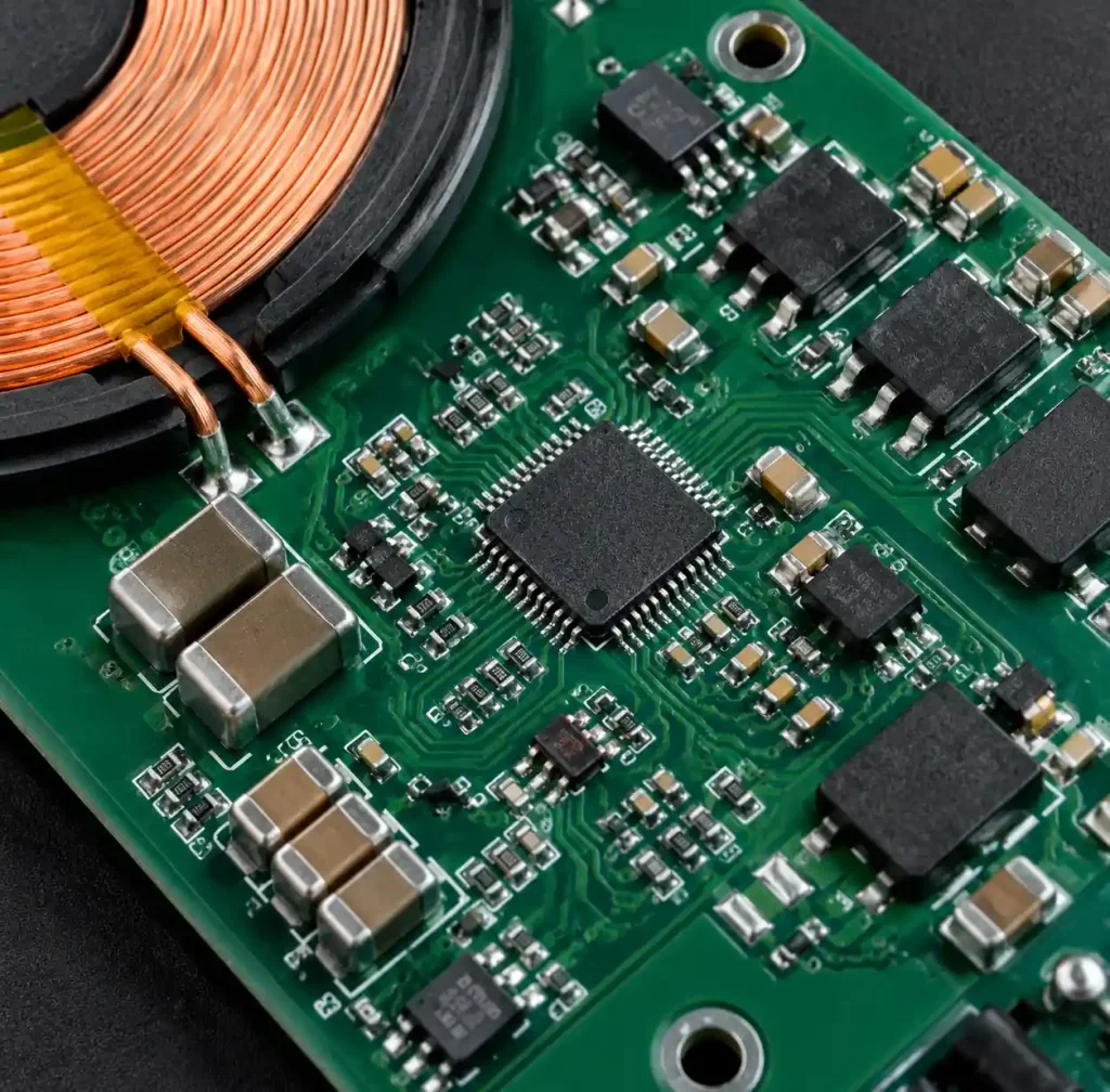
Qi-compliant controller ICs manage power regulation, communication protocol, and foreign object detection. PCB layout around the controller determines overall system performance.
Component placement: Position the controller IC within 10-15 mm of the coil connection point to minimize trace inductance. Place resonant capacitors within 3-5 mm of coil terminals. Use 0.3-0.5 mm traces for high-frequency signals to reduce parasitic inductance below 10 nH.
Ground plane strategy: Dedicate one PCB layer as continuous ground. Connect coil center tap, controller ground, and power ground at a single star point to prevent ground loops. Separate analog ground (controller sense pins) from power ground (MOSFET source) using ferrite beads or 0Ω resistors.
Decoupling network: Place 10 μF bulk capacitors within 20 mm and 0.1 μF ceramic capacitors within 2 mm of controller power pins. Add 1-10 nF capacitors across sensitive analog pins. Follow controller datasheet recommendations for resonant tank values—typically 100-470 nF for TX coils and 47-220 nF for RX coils.
Foreign Object Detection (FOD) Design Requirements
FOD prevents wireless chargers from heating coins, keys, or metal objects placed between coils. Qi standards mandate FOD response within 50 ms of object detection.
Detection methods: Power-loss FOD compares TX power sent versus RX power received. Discrepancies above 2-3W indicate foreign objects. Q-factor FOD measures coil quality factor changes when metal objects enter the field. Qi 2.2 requires both methods for 25W certification.
PCB design impact: FOD requires accurate current sensing. Use 0.1% tolerance sense resistors (typically 5-20 mΩ) with Kelvin connections. Route sense traces as differential pairs with controlled impedance to minimize noise pickup. Place sense resistors within 30 mm of the controller ADC pins.
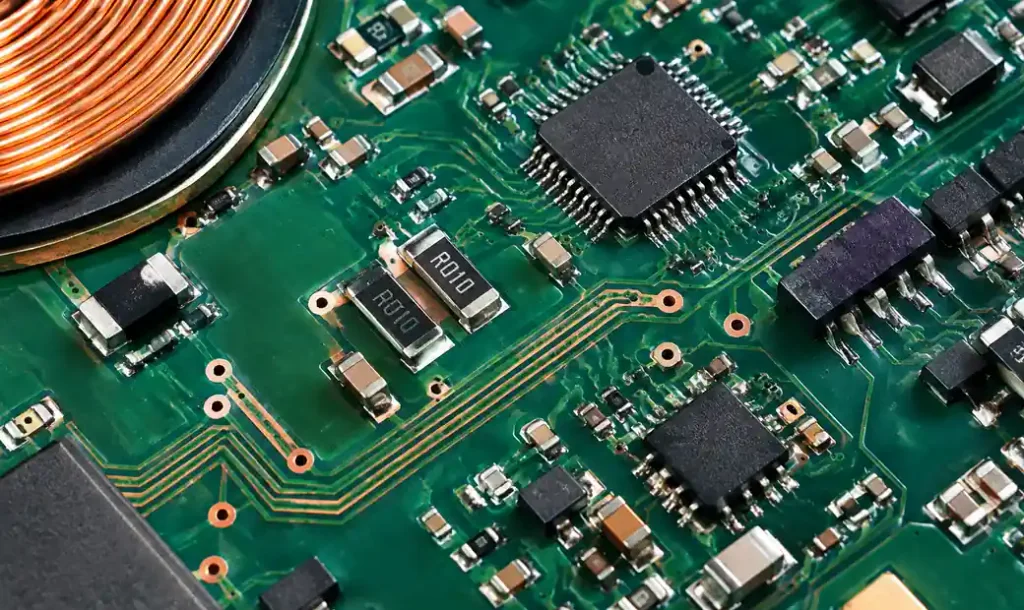
Calibration considerations: FOD accuracy depends on coil inductance tolerance. Specify ±5% inductance tolerance through controlled PCB manufacturing. Use IPC-6012 Class 2 or higher with ±10% trace width control for consistent coil performance across production batches.
Transmitter vs Receiver Coil Design Differences
TX and RX coils serve different functions and require distinct PCB approaches.
| Parameter | Transmitter (TX) Coil | Receiver (RX) Coil |
|---|---|---|
| Inductance | 10-25 μH | 5-15 μH |
| Turns | 15-25 turns | 10-18 turns |
| Copper weight | 2-4 oz (70-140 μm) | 1-2 oz (35-70 μm) |
| Current handling | 2-4A peak | 1-2A peak |
| Coil diameter | 60-80 mm (pad size) | 40-60 mm (phone size) |
| Ferrite thickness | 0.3-0.5 mm | 0.1-0.3 mm |
| PCB layers | 4-6 layers recommended | 2-4 layers sufficient |
TX coil considerations: Transmitter coils in charging pads must handle higher currents and power dissipation. Use 2-4 oz copper with 0.5-0.8 mm trace width. Implement active cooling (fans) or passive heatsinks for 15-25W designs. TX boards benefit from multilayer PCB stackups with dedicated power and ground planes.
RX coil considerations: Receiver coils in phones prioritize thin form factors. Single or double-layer flex PCB designs reduce thickness to 0.2-0.4 mm. Use polyimide substrates for flexibility around batteries. Position RX coils to avoid interference with cameras, NFC antennas, and display connectors.
Design for Manufacturing (DFM) and Testing
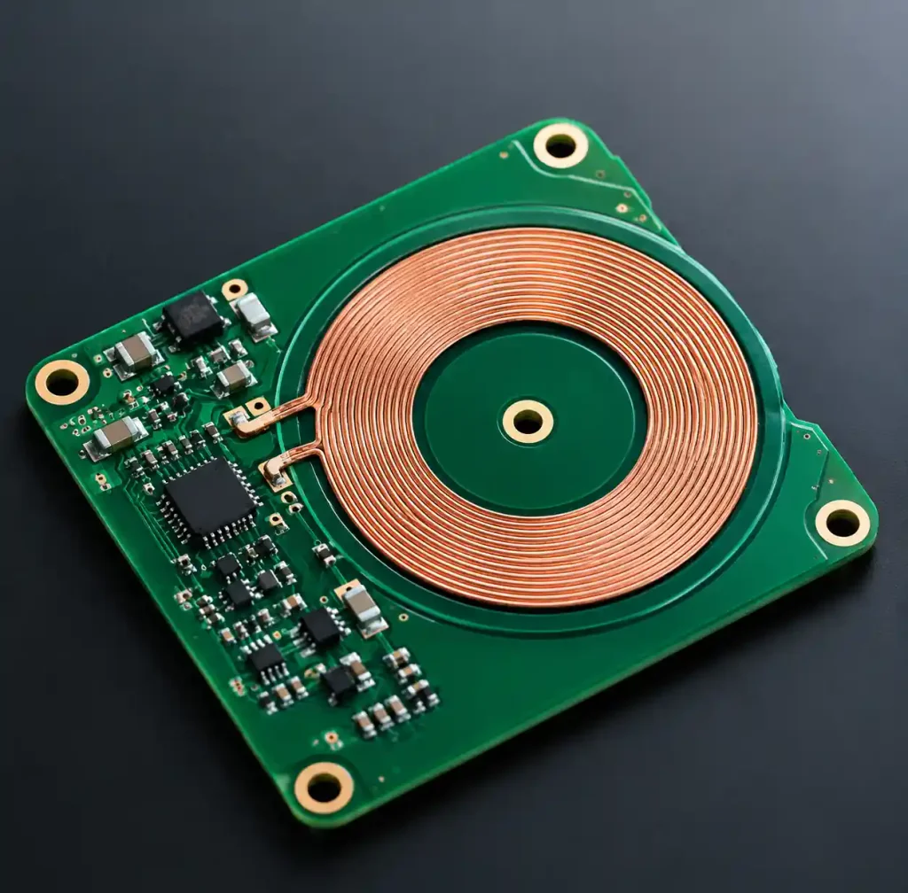
Wireless charging PCBs require tight manufacturing tolerances for consistent coil performance.
Trace width and spacing control: Specify ±10% trace width tolerance per IPC-6012 Class 2. Wider tolerances cause inductance variation exceeding ±15%, affecting power transfer efficiency. Use DFM guidelines to verify trace width, spacing, and coil geometry before fabrication.
Impedance testing: For designs with 50Ω controller traces, request TDR impedance testing with ±10% tolerance. Include test coupons on production panels to verify impedance across manufacturing batches.
Inductance verification: Test coil inductance at 100 kHz using LCR meters. Target ±5% tolerance from design value. Inductance shifts above ±10% indicate trace width errors or copper thickness variation. Specify copper weight tolerance of ±10% in fabrication notes.
Qi certification testing: Products require Wireless Power Consortium (WPC) certification for Qi branding. Testing includes power transfer efficiency (minimum 70%), FOD response time, EMI compliance per FCC/CE, and interoperability with certified chargers. Allocate 4-8 weeks for certification testing and potential design iterations.
Application Examples and Design Approaches
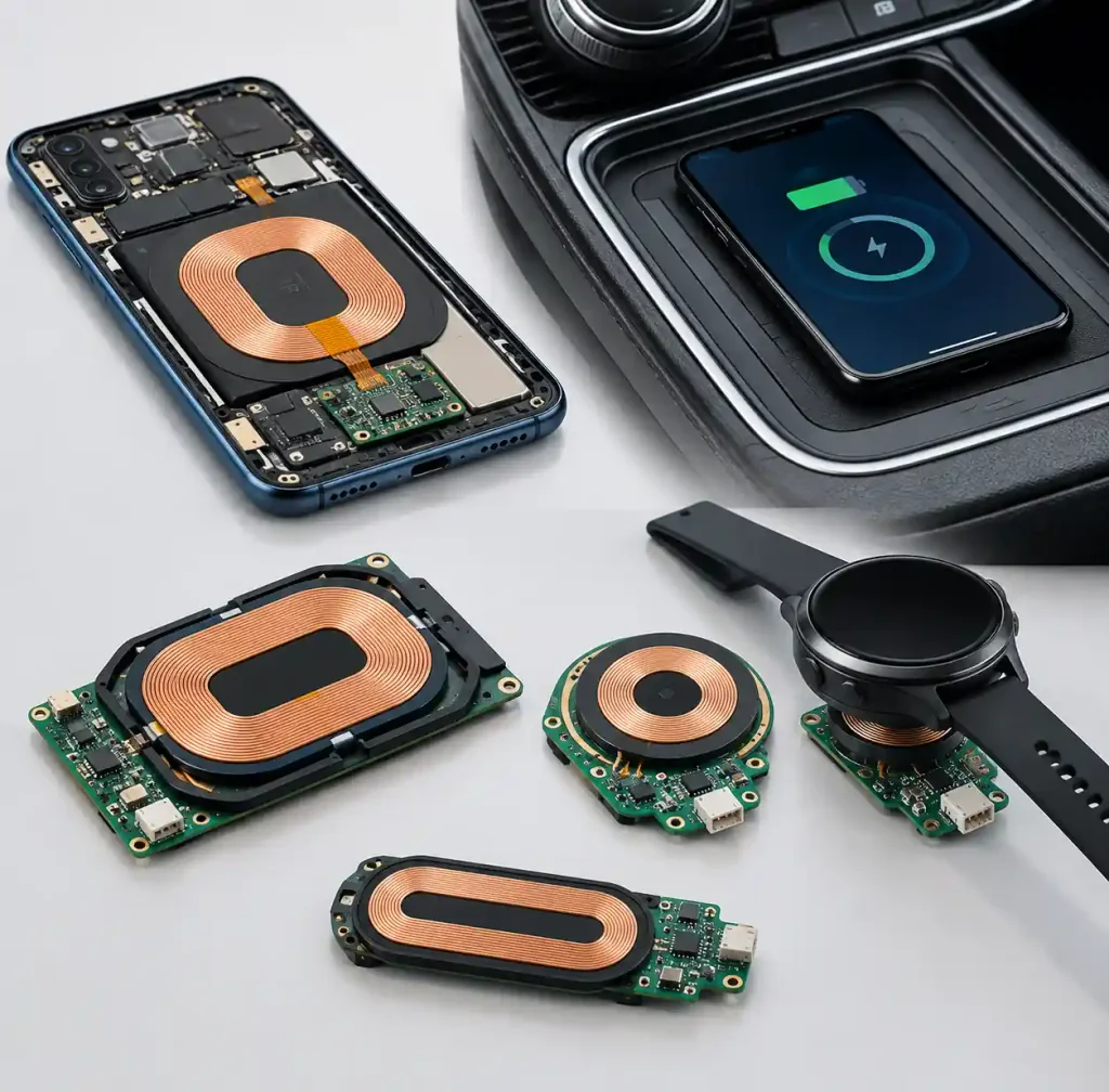
Smartphone wireless charging: Flagship phones use 15-25W RX coils integrated into 2-4 layer flex-rigid PCBs. iPhone 17 implements Qi 2.2 with magnetic alignment rings (15 small magnets around coil perimeter) for precise positioning. Design requires 55-60 mm diameter coils with 0.2 mm polyimide flex circuits, 1 oz copper, and 0.15 mm ferrite backing.
Automotive wireless charging: In-vehicle charging pads deliver 15W sustained power in -40°C to +85°C environments. Use FR-4 with Tg 180°C, 4-layer stackup, 2 oz copper, and 0.3 mm ferrite. Follow automotive PCB standards including AEC-Q200 qualification and IATF 16949 manufacturing certification.
Wearable device charging: Smartwatches use 5W RX coils as small as 20-30 mm diameter. These require precise coil alignment through mechanical guides or MPP magnetic rings. Single-layer designs with 0.5 oz copper and 0.1 mm ferrite minimize thickness while meeting power requirements for 200-400 mAh batteries.
Wireless Charging PCB Design Checklist
Before finalizing your design:
- Verify coil inductance calculation matches target (5-15 μH RX, 10-25 μH TX)
- Confirm copper weight supports current requirements (2-4A for TX, 1-2A for RX)
- Add ferrite backing with 3-5 mm margin beyond coil outer diameter
- Place controller IC within 10-15 mm of coil connection
- Implement thermal vias beneath controller and power components
- Route sense resistor traces as differential pairs with Kelvin connections
- Specify ±10% trace width tolerance in fabrication drawings
- Include test points for coil inductance and DC resistance measurement
- Verify EMI shielding meets FCC Part 15 and CE requirements
- Plan for WPC certification testing (4-8 weeks lead time)
Frequently Asked Questions
What PCB thickness works for wireless charging coils?
Standard 1.6 mm (63 mil) thickness works for most wireless charging applications. Transmitter coils in charging pads use 1.6-2.0 mm boards for rigidity. Receiver coils in smartphones often use 0.2-0.8 mm flex or rigid-flex PCBs to minimize device thickness. Thinner boards require careful handling during assembly to prevent warpage.
Can I use standard FR-4 for 25W Qi 2.2 designs?
Standard FR-4 with Tg 130-140°C works for 5-10W applications. For 15W designs, specify Tg 170°C minimum. Qi 2.2’s 25W power transfer generates significant heat requiring Tg 180-200°C materials or polyimide for sustained operation without delamination. High-Tg materials add 15-25% cost but prevent field failures from thermal stress.
How does coil diameter affect charging efficiency?
Larger coils capture more magnetic flux, improving coupling coefficient and efficiency. However, coil diameter is limited by device size. Optimal RX coil diameter is 70-80% of the TX coil diameter for maximum coupling. A 40 mm RX coil achieves 85% efficiency with a 55 mm TX coil, but only 70% efficiency with an 80 mm TX coil due to increased leakage flux.
What copper weight should I specify for wireless charging PCB?
Use 1 oz (35 μm) copper for 5W RX coils, 2 oz (70 μm) for 10-15W designs, and 3-4 oz (105-140 μm) for 25W Qi 2.2 applications. Heavier copper reduces DC resistance and I²R losses but requires wider trace spacing. A 15W design with 2 oz copper achieves 88% efficiency versus 82% with 1 oz copper, justifying the 20-30% cost increase.
Do wireless charging PCBs require special stackup design?
Simple 2-layer stackups work for RX coils under 10W. TX coils and higher-power designs benefit from 4-layer stackups with dedicated power and ground planes for better EMI shielding and thermal spreading. Use controlled impedance stackups when controller outputs require 50Ω matching. Multi-layer designs add 40-60% cost but improve reliability and certification success rates.
How do I calculate the required number of coil turns?
Target inductance determines turn count. Use the formula: L ≈ (μ₀ × μᵣ × N² × A) / l, where N is turns, A is coil area, and l is coil length. For a 50 mm diameter RX coil targeting 10 μH with ferrite backing (μᵣ = 200), you need approximately 12-15 turns with 0.5 mm trace width and 0.3 mm spacing. Use online inductance calculators or electromagnetic simulation tools for precise values.
Conclusion
PCB coil design for wireless charging demands precise control of trace geometry, copper weight, ferrite shielding, and thermal management to meet Qi 2.2 standards. Proper design achieves 85-90% efficiency while supporting 15-25W power transfer in compact form factors. Focus on controller integration, FOD implementation, and DFM practices to ensure certification success and field reliability.
If you need wireless charging PCB manufacturing for your consumer electronics or automotive project, Andwin Circuits offers advanced capabilities including controlled impedance, heavy copper up to 6 oz, and flex-rigid construction. Our ISO 9001 and IATF 16949 certified manufacturing ensures Qi-compliant boards with fast delivery in 7-15 days.
Contact us today for custom wireless charging PCB solutions with factory-direct pricing and engineering support.