
PCB Prototype to Production: Scaling Design for Manufacturing (DFM)
Transitioning from PCB prototype to mass production creates a critical inflection point where design-related manufacturing problems account for 40% of production failures. The average NPI (New Product Introduction) cycle extends 8-12 weeks due to DFM oversights not caught during prototyping.
This guide covers the complete transition strategy including DFM optimization, cost reduction methods, testing strategies, and yield improvement approaches for 99%+ first-pass success rates.
What Is PCB Prototype to Production Transition?
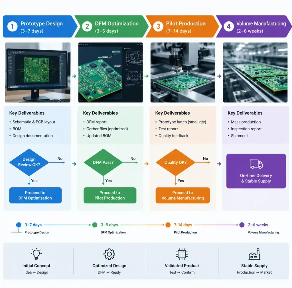
PCB prototype to production transition is the systematic process of scaling validated circuit board designs from low-volume prototyping (10-100 units) to high-volume manufacturing (1,000+ units) while optimizing cost, yield, and manufacturability through comprehensive DFM analysis, panel utilization optimization, component verification, and testing strategy development.
A prototype proves your design works electrically. Production engineering ensures that design can be built repeatedly at target cost and quality without manual intervention or rework.
Key Differences: Prototype vs Production PCB
Understanding the distinctions between prototype and production requirements helps you design correctly from the start.
| Aspect | Prototype PCB | Production PCB |
|---|---|---|
| Volume | 10-100 units | 1,000-100,000+ units |
| Lead Time | 3-7 days | 15-30 days (includes tooling) |
| Cost Per Board | $50-500 | $5-50 (volume dependent) |
| Panel Utilization | Single or minimal | Optimized for maximum yield |
| Testing | Flying probe or manual | ICT fixture + AOI + functional test |
| Component Sourcing | Authorized distributors | Direct factory, long-lead planning |
| Design Changes | Frequent iterations | Frozen after validation |
| Quality Standard | IPC Class 2 acceptable | IPC Class 3 for high reliability |
DFM Optimization: From Prototype to Production
Design for Manufacturing optimization transforms a working prototype into a production-ready design by addressing manufacturing constraints before volume production.
Panel Utilization Strategy
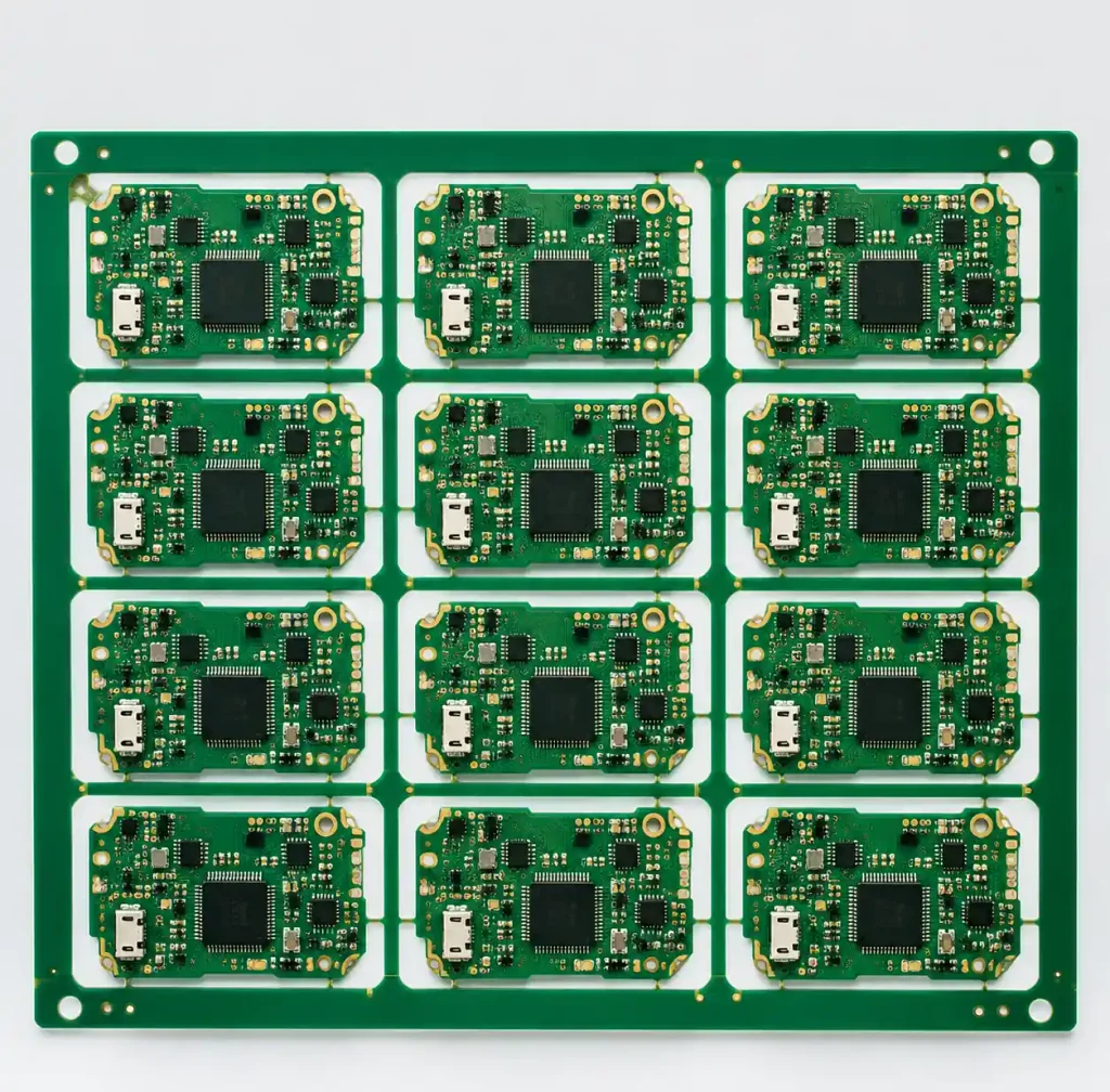
Panel utilization directly impacts per-board manufacturing cost. Production PCBs are manufactured on standardized panel sizes, typically 18″ × 24″ (457mm × 610mm). Optimizing board fit reduces material waste and increases throughput.
For a 100mm × 150mm board on an 18″ × 24″ panel, you can fit approximately 16-20 boards depending on separation method. Poor panel design wastes 30-40% of material cost. Work with your PCB manufacturer to optimize array configuration and tooling hole placement. Learn more about PCB panelization strategies.
Component Placement and Assembly Optimization
Component placement directly affects assembly yield and cost. Production assembly uses automated pick-and-place machines requiring consistent component orientation, adequate clearance, and accessible test points.
Critical DFM rules:
- Component orientation: Align all polarized components in the same direction
- Assembly clearance: Maintain 5mm from board edge, 3mm around tooling holes
- Test point access: Place test points on 100mil grid, minimum 40mil pad diameter
- Fiducial marks: Include 3 global fiducials (1mm copper circles) at board corners
These rules prevent pick-and-place alarms and enable 99.5%+ first-pass success. See our PCB assembly services guide.
Design Rule Verification
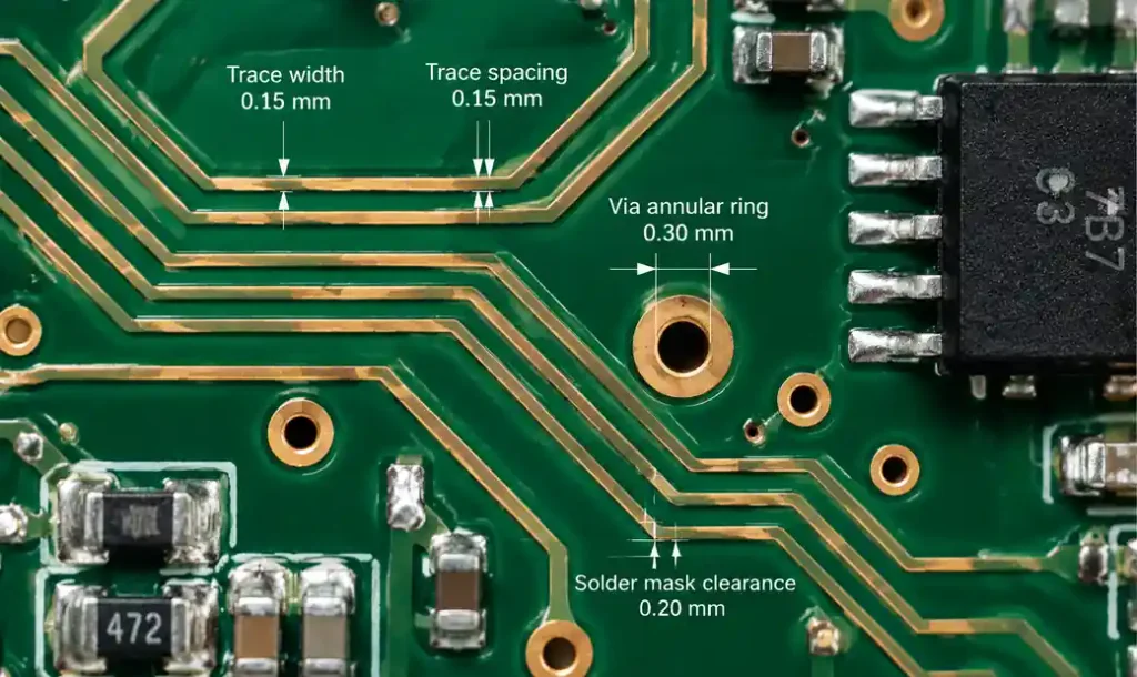
Production facilities enforce tighter tolerances than prototype shops. Your design must meet manufacturer minimum capabilities for trace width, spacing, hole sizes, and annular rings.
| Design Parameter | Prototype | Production | High-Reliability |
|---|---|---|---|
| Min Trace/Space | 4/4 mil | 5/5 mil | 6/6 mil |
| Min Drill Size | 0.15mm | 0.2mm | 0.25mm |
| Annular Ring | 2 mil | 3 mil | 4 mil |
| Aspect Ratio | 12:1 | 10:1 | 8:1 |
Designing to production-standard rules rather than prototype minimums reduces PCB manufacturing cost by 20-30%. Review our PCB DFM checklist before finalizing designs.
Cost Reduction Strategies for Production
Transitioning from prototype to production enables significant per-board cost reduction through volume economies and design optimization.
Material and Layer Count Optimization
PCB cost scales exponentially with layer count. Reducing from 8 to 6 layers cuts board cost by 35-45%, while 4-layer designs cost 60-70% less than 6-layer equivalents.
Layer count reduction techniques:
- Use multi-function ICs to reduce routing complexity
- Utilize blind and buried vias only where essential
- Improve trace routing to eliminate unnecessary signal layers
Evaluate layer count reduction during prototype validation. If your 8-layer prototype has 30% routing utilization per signal layer, you can consolidate to 6 layers. Learn more about PCB layer stackup design.
Standard Materials and Processes
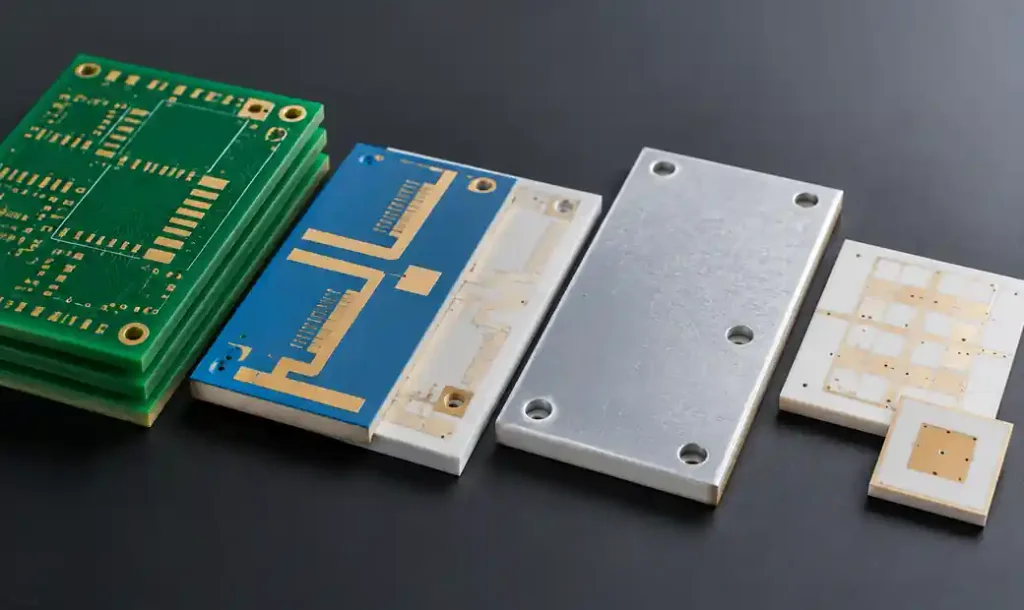
Specifying standard materials significantly reduces cost. FR-4 TG150-170 covers 90% of commercial applications. High-frequency Rogers materials, polyimide, or aluminum cores should only be specified when thermal or RF requirements demand them.
Material cost impact:
- Standard FR-4: Baseline
- High-Tg FR-4: +15-25%
- Rogers RO4003C: +200-300%
Standard surface finishes (HASL, ENIG) cost less than specialty finishes. Compare PCB surface finish options for your application.
Volume Commitment and Supplier Negotiation
Production volume enables price negotiation with volume discounts:
- 500-1,000 units: 10-15% discount
- 1,000-5,000 units: 20-30% discount
- 5,000+ units: 30-45% discount
Secure better pricing by committing to annual volumes and accepting longer lead times.
Testing Strategy: Prototype to Production
Testing strategy evolves as production volume increases. The goal is maximum defect coverage at minimum cost per board.
Flying Probe for Prototypes and NPI
Flying probe testing uses movable probes controlled by software to verify electrical connections without custom fixturing. This flexibility makes flying probe ideal for prototypes and early production where design changes are frequent.
Flying probe advantages:
- No fixture cost (saves $3,000-8,000)
- Rapid test program generation
- Accommodates design changes through software updates
- 85-92% fault coverage
Use flying probe during prototype validation and first production runs up to 500-1,000 units. Learn more about quick turn PCB assembly for prototype testing.
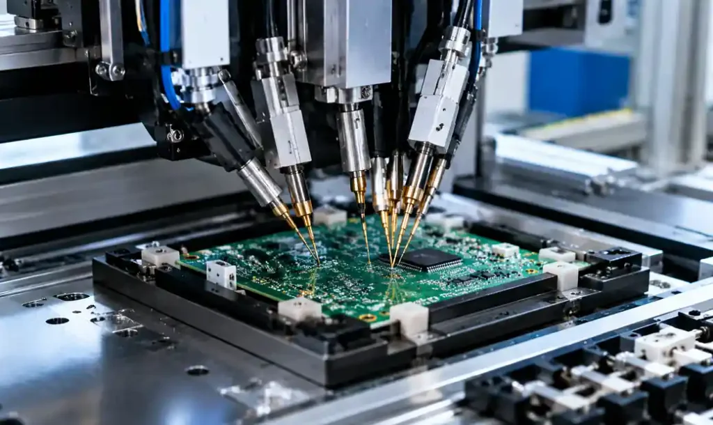
In-Circuit Test (ICT) for Volume Production
ICT uses a custom “bed of nails” fixture with spring-loaded probes positioned to contact specific test points. Once manufactured, ICT provides fast, repeatable testing at production volumes.
ICT advantages:
- Rapid test execution (20-60 seconds per board)
- 95-98% fault coverage with proper test point design
- Low per-board cost at volume ($0.50-2.00)
ICT requirements:
- Custom fixture cost ($3,000-8,000, 3-4 week lead time)
- Design must include adequate test points
Break-even occurs at 800-1,500 units depending on complexity. For details, see our guide on PCB E-test methods.
Combined Testing Strategy
Production testing often combines multiple methods for comprehensive coverage:
- AOI (Automated Optical Inspection): Catches placement errors, solder bridges, and missing components
- ICT or Flying Probe: Verifies electrical connectivity and component values
- Functional Test: Validates end-to-end operation
This layered approach achieves 99.5%+ defect detection while maintaining production throughput.
Component Sourcing and Supply Chain
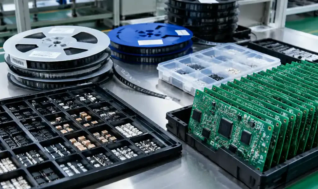
Component availability becomes critical when scaling from prototype to production. Parts readily available in prototype quantities may have 12-26 week lead times at production volumes.
Long-Lead Component Planning
Identify long-lead components early. Power management ICs, specialized sensors, and RF modules frequently have 16-24 week factory lead times.
- Verify production availability: Check manufacturer stock for production quantities
- Plan component procurement: Order long-lead components before PCB fabrication
- Design with alternatives: Include footprint compatibility for second-source components
Component lead time mismatches cause 60% of NPI schedule delays.
NPI Process and Pilot Production
New Product Introduction bridges the gap between prototype validation and full production. This phase validates manufacturing processes, identifies yield issues, and establishes quality baselines.
Pilot Run Strategy
A pilot production run of 50-200 units validates processes before volume commitment:
- Process validation: Verify assembly equipment and test procedures work correctly
- Yield baseline: Measure first-pass yield and identify failure modes
- Documentation verification: Confirm assembly drawings and quality standards are complete
The pilot run should use production tooling to accurately represent volume manufacturing conditions.
Yield Improvement Techniques
Production yield typically starts at 85-92% during pilot runs and improves to 98-99.5% as processes stabilize.
| Defect Type | Impact | Solution |
|---|---|---|
| Solder bridging | 15-25% | Optimize stencil apertures, improve pad design |
| Placement errors | 10-18% | Fix fiducial placement, verify orientation |
| Missing components | 8-12% | Improve tape-and-reel feeding, add AOI |
| Cold solder joints | 12-20% | Optimize reflow profile, verify thermal mass |
| Tombstoning | 8-15% | Balance pad sizes, adjust paste volume |
Systematic analysis during pilot production eliminates these issues before volume manufacturing begins.
Andwin Circuits: Prototype to Production Expertise
Andwin Circuits specializes in the complete prototype-to-production transition with manufacturing capabilities up to 50 layers and fast delivery in 7 days for prototypes. Our DFM analysis identifies cost and yield optimization opportunities before production tooling.
Our facility holds ISO 9001, IATF 16949, and UL certifications, ensuring quality for automotive, medical, telecommunications, and industrial applications. We provide turnkey PCB assembly including component sourcing, SMT assembly, testing, and conformal coating.
We achieve 99%+ first-pass yields through systematic DFM optimization. Explore our PCB manufacturing capabilities and HDI PCB services.
FAQ
Q: When should I transition from prototype to production PCB manufacturing?
Transition once your design is validated and frozen, component availability is confirmed for production volumes, and your forecast exceeds 500-1,000 units. Earlier transition wastes money on tooling that becomes obsolete with design changes.
Q: How much cost reduction is possible moving from prototype to production?
Per-board cost typically decreases 60-80% from prototype (10-50 units) to production volumes (5,000+ units). A $100 prototype board commonly costs $20-40 in production due to volume pricing and panel optimization.
Q: What is the typical timeline for prototype to production transition?
Expect 8-12 weeks including DFM optimization (1-2 weeks), pilot run and testing (3-4 weeks), yield improvement (2-3 weeks), and production ramp-up (2-3 weeks).
Q: What testing strategy should I use when scaling to production?
Use flying probe for prototypes and first builds (up to 500-1,000 units). Invest in ICT fixture once design is frozen and volume exceeds 800-1,500 units. Combine electrical testing with AOI and functional testing.
Q: How do I optimize panel utilization to reduce cost?
Work with your PCB manufacturer to arrange multiple boards per panel, select efficient separation method, minimize spacing, and use standard panel sizes. Proper panel design reduces material cost by 25-40%.
Conclusion
Successfully scaling PCB designs from prototype to production requires systematic DFM optimization, cost reduction strategies, and manufacturing validation. Treat this transition as a distinct engineering phase rather than simply ordering larger quantities.
Focus on optimizing design for manufacturing consistency, establishing robust testing strategies that scale with volume, and validating processes through pilot production. Companies that invest in proper DFM analysis achieve 99%+ yields and reduce per-board costs by 60-80%.
Contact us today for custom PCB solutions, DFM analysis, and competitive pricing for your prototype-to-production transition.