A brief discussion of circuit board design criteria to ensure signal integrity
The earlier the signal integrity (SI) problem is solved, the more efficient the design will be, thus avoiding the need to add termination devices after the circuit board design is completed. There are many tools and resources for SI design planning. This article explores the core issues of signal integrity and several methods to solve SI problems, ignoring the technical details of the design process.
1 Introduction of SI problems
With the increase in IC output switching speed, almost all designs have encountered signal integrity problems regardless of the signal cycle. Even if you have not encountered SI problems in the past, you will definitely encounter signal integrity problems in the future as the circuit operating frequency increases.
Signal integrity problems mainly refer to signal overshoot and damped oscillation phenomena, which are mainly functions of IC drive amplitude and jump time. In other words, even if the wiring topology does not change, as long as the chip speed becomes fast enough, the existing design will be in a critical state or stop working. We use two examples to illustrate that signal integrity design is inevitable.
In the field of communications, cutting-edge telecommunications companies are producing high-speed circuit boards (above 500MHz) for voice and data exchange. At this time, cost is not particularly important, so multi-layer boards can be used as much as possible. Such a circuit board can achieve full grounding and easily form a power loop. A large number of discrete termination devices can also be used as needed, but the design must be correct and cannot be in a critical state.
SI and EMC experts must perform simulations and calculations before wiring.
Then, the circuit board design can follow a series of very strict design rules. In doubtful places, termination devices can be added to obtain as much SI safety margin as possible. There will always be some problems in the actual operation of the circuit board. For this reason, SI problems can be avoided by adopting controlled impedance termination wiring. In short, super-standard design can solve SI problems.
The following introduces the general SI design principles of the design process.
2 Preparations before design
(1)Thinking about determine the design strategy.
Before the design begins, it is necessary to think about and determine the design strategy in advance, so as to guide tasks such as component selection, process selection and circuit board production cost control. As far as SI is concerned, it is necessary to conduct research in advance to form a plan or design criteria to ensure that the design results do not have obvious SI problems, crosstalk or timing problems. Some design guidelines can be provided by IC manufacturers. However, the guidelines provided by chip suppliers (or the guidelines you design yourself) have certain limitations. According to such guidelines, it may not be possible to design a circuit board that meets SI requirements. If the design rules are easy, there is no need for design engineers.
Before the actual wiring, the following issues must be solved first. In most cases, these issues will affect the circuit board you are designing (or considering designing). If the number of circuit boards is large, this work is valuable.

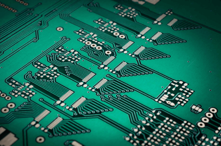
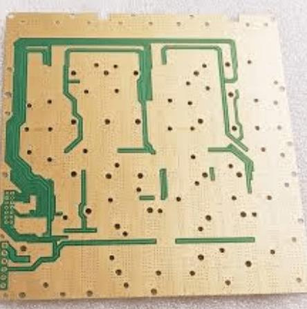
3 Circuit board stacking
Some project groups have great autonomy in determining the number of PCB layers, while others do not have this autonomy. Therefore, it is important to understand your position. Communication with manufacturing and cost analysis engineers can determine the stacking error of the circuit board. This is also a good opportunity to discover the manufacturing tolerance of the circuit board. For example, if you specify that a certain layer is 50Ω impedance control, how does the manufacturer measure and ensure this value?
Other important questions include:
What is the expected manufacturing tolerance?
What is the expected insulation constant on the circuit board?
What is the allowable error of line width and spacing?
What is the allowable error of the thickness and spacing of the ground layer and signal layer? All this information can be used in the pre-wiring stage.
Based on the above data, you can choose the stackup. Note that almost every PCB that plugs into another board or backplane has a thickness requirement, and most board manufacturers have fixed thickness requirements for the different types of layers they can manufacture, which will greatly constrain the number of final stackups. You may be tempted to work closely with the manufacturer to define the number of stackups. Impedance control tools should be used to generate target impedance ranges for the different layers, making sure to consider the manufacturing tolerances provided by the manufacturer and the effects of adjacent routing.
In an ideal situation where the signal is intact, all high-speed nodes should be routed on impedance-controlled inner layers (such as striplines), but in reality, engineers must often use outer layers to route all or some high-speed nodes. To optimize SI and keep the board decoupled, ground/power planes should be placed in pairs whenever possible. If you can only have one ground/power pair, you will have to make do. If there are no power planes at all, you may have SI problems by definition. You may also encounter situations where it is difficult to simulate or emulate the performance of the board before the return path for the signal is defined.

4 Crosstalk and Impedance Control
Coupling from adjacent signal lines will cause crosstalk and change the impedance of the signal line. Coupling analysis of adjacent parallel signal lines may determine the “safe” or expected spacing (or parallel routing length) between signal lines or between types of signal lines. For example, if you want to limit the crosstalk from the clock to the data signal node to less than 100mV, but keep the signal traces parallel, you can find the minimum allowable spacing between signals on any given routing layer through calculation or simulation. At the same time, if the design contains impedance-critical nodes (either clocks or dedicated high-speed memory architectures), you must place the routing on a layer (or several layers) to achieve the desired impedance.
5 Important high-speed nodes
Delay and skew are key factors that must be considered in clock routing. Because of the strict timing requirements, such nodes usually require termination devices to achieve the best SI quality. Predetermine these nodes and plan the time required to adjust component placement and routing to adjust the pointers of signal integrity design.
6 Technology selection
Different drive technologies are suitable for different tasks. Is the signal point-to-point or point-to-multiple taps? Is the signal output from the board or stays on the same board? What is the allowed skew and noise margin? As a general rule of thumb for signal integrity design, the slower the transition speed, the better the signal integrity. There is no reason to use a 500PS rise time for a 50MHZ clock. A 2-3NS slew rate control device must be fast enough to ensure SI quality and help solve problems such as output synchronous switching (SSO) and electromagnetic compatibility (EMC).
The advantages of drive technology can be found in new FPGA programmable technology or user-defined ASICs. With these custom (or semi-custom) devices, you have a lot of room to select drive amplitude and speed. In the early stages of design, meet the requirements of FPGA (or ASIC) design time and determine the appropriate output selection, including pin selection if possible.
At this stage of design, obtain appropriate simulation models from IC suppliers. In order to effectively cover SI simulation, you will need an SI simulation program and corresponding simulation models (possibly IBIS models).
Finally, you should establish a series of design guidelines in the pre-routing and routing stages, which include: target layer impedance, routing spacing, preferred device technology, important node topology and termination planning.
7 Pre-wiring stage
The basic process of pre-wiring SI planning is to first define the input parameter range (drive amplitude, impedance, tracking speed) and possible topology range (minimum/maximum length, short line length, etc.), then run each possible simulation combination, analyze the timing and SI simulation results, and finally find an acceptable range of values.
Next, interpret the working range as the routing constraints for PCB routing. Different software tools can be used to perform this type of “cleaning” preparation, and the routing program can automatically handle such routing constraints. For most users, timing information is actually more important than SI results. The results of interconnect simulation can change the routing and adjust the timing of the signal path.
In other applications, this process can be used to determine the placement of pins or devices that are incompatible with the system timing pointer. At this point, it is possible to completely determine the nodes that need to be manually routed or the nodes that do not need termination. For programmable devices and ASICs, the output drive selection can also be adjusted at this time to improve the SI design or avoid the use of discrete termination devices.
8 Post-wiring SI simulation
In general, SI design guidelines are difficult to guarantee that there will be no SI or timing problems after the actual routing is completed. Even if the design is guided by guidelines, unless you can continuously and automatically check the design, there is no way to ensure that the design fully complies with the guidelines, and problems are inevitable. Post-layout SI simulation checks will allow planned breaking (or changing) of design rules, but this is only necessary for cost considerations or strict wiring requirements.
9 Post-manufacturing stage
Taking the above measures can ensure the SI design quality of the circuit board. After the circuit board assembly is completed, it is still necessary to put the circuit board on the test platform and use an oscilloscope or TDR (time domain reflectometer) to measure and compare the actual circuit board with the expected results of the simulation. These measurement data can help you improve the model and manufacturing parameters so that you can make better (less constrained) decisions in the next pre-design investigation.
10 Model selection
There are many articles on model selection. Engineers who perform static timing verification may have noticed that although all the data can be obtained from the device data sheet, it is still difficult to build a model. SI simulation models are just the opposite. The model is easy to build, but the model data is difficult to obtain. In essence, the only reliable source of SI model data is IC suppliers, who must maintain tacit cooperation with design engineers. The IBIS model standard provides a consistent data carrier, but the establishment of IBIS models and the assurance of their quality are costly. IC suppliers still need the impetus of market demand to make this investment, and circuit board manufacturers may be the only demand-side market.