Advanced Stencil PCB Assembly Strategies for Reliable Production
Key Takeaways
Effective PCB assembly relies on strategic integration of design, material science, and process control. For stencil PCB assembly, three pillars define success: solder paste optimization, precision alignment, and data-driven quality assurance. Modern PCBA workflows demand rigorous attention to stencil aperture geometries, which directly influence solder volume consistency.
"A 5% variation in solder paste deposition can lead to a 15% increase in defects—underscoring the need for micrometer-level stencil accuracy."
| Factor | Optimization Strategy | Impact on Yield |
|---|---|---|
| Aperture Design | Laser-cut, nano-coated stencils | +12% |
| Paste Viscosity | Dynamic temperature control | +8% |
| Cleaning Frequency | Automated inline systems | +10% |
Critical considerations include thermal profiling to prevent voiding and tombstoning, paired with real-time SPI (Solder Paste Inspection) systems. For high-reliability PCBA, prioritize stencils with ≥95% transfer efficiency and materials resistant to wear-induced deformation.
Pro Tip: Validate process parameters using DOE (Design of Experiments) to isolate variables affecting solder joint integrity. This approach reduces rework rates by 20–30% in mixed-technology assemblies.
Transitioning to automated stencil cleaning eliminates residue-driven defects like bridging, while adaptive algorithms in PCB assembly lines enable predictive adjustments for humidity and temperature shifts. Always align defect prevention protocols with IPC-A-610 standards for auditable compliance.
Solder Paste Optimization Techniques for PCB Assembly
Effective solder paste optimization is foundational to achieving high-quality pcb assembly outcomes. The viscosity and composition of the paste directly influence printability and wetting behavior, with modern formulations balancing lead-free alloys and flux chemistry to meet environmental regulations while ensuring robust electrical connections. For pcba applications, precise control over aperture fill rates (typically 75–85%) minimizes voids and bridging, particularly in fine-pitch components.
Critical parameters include stencil design alignment with pad geometries, paste volume consistency, and reflow profile compatibility. Advanced rheology modifiers enable tailored flow characteristics, reducing defects like solder balling or insufficient joints. Real-time monitoring systems now integrate 3D solder paste inspection (SPI) to validate deposition accuracy, feeding data back to stencil printers for dynamic adjustments.
Optimization extends to environmental factors: humidity-controlled storage preserves paste integrity, while temperature-stabilized printing chambers maintain dynamic viscosity during high-volume pcb assembly. By combining material science with process analytics, manufacturers achieve first-pass yield improvements of 15–30% in pcba workflows, directly enhancing end-product reliability.
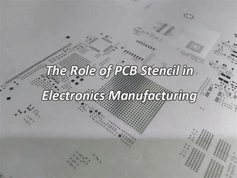
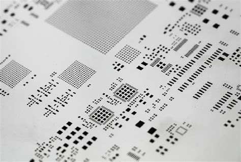
Precision Stencil Design for Defect-Free PCB Assembly
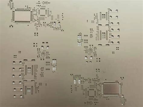
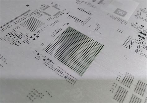
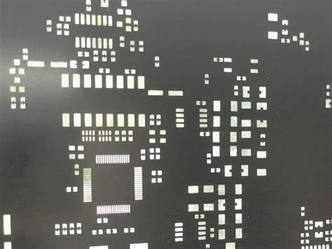
Achieving defect-free PCB assembly begins with optimizing stencil design, a critical determinant of solder paste deposition accuracy. Aperture geometry, stencil thickness, and alignment precision directly influence solder volume consistency, which is pivotal for avoiding common PCBA flaws like bridging, insufficient solder, or tombstoning. Modern designs leverage laser-cut or electroformed stencils with trapezoidal apertures to improve paste release, particularly for high-density interconnect (HDI) boards. For mixed-technology assemblies, step stencils with varying thickness zones ensure optimal paste deposition for both fine-pitch BGA components and larger through-hole connectors.
Material selection further impacts performance: stainless steel remains the standard for durability, while nano-coated stencils reduce cleaning frequency by up to 40% in high-volume PCB assembly lines. Advanced SMT workflows integrate 3D stencil inspection systems to verify aperture dimensions within ±2µm tolerances, aligning with IPC-7525D standards. Real-time process feedback loops adjust stencil positioning using vision-guided systems, minimizing misregistration risks during double-sided PCBA. By prioritizing these design principles, manufacturers reduce rework rates by 15–25% while maintaining IPC Class 3 reliability thresholds for mission-critical applications.
Process Control Strategies in SMT Manufacturing
Effective process control in PCB assembly requires meticulous management of variables affecting solder joint formation and component placement accuracy. Real-time monitoring systems track critical parameters such as solder paste deposition thickness (typically 100-150µm) and component placement precision (±25µm tolerance), enabling immediate adjustments during PCBA production. Closed-loop feedback mechanisms integrate data from automated optical inspection (AOI) and solder paste inspection (SPI) systems to detect deviations like insufficient paste volume or misaligned components, reducing defect rates by up to 40% in high-volume runs.
Environmental controls maintain optimal conditions for stencil printing and reflow processes, with temperature stability (±1.5°C) and humidity levels (30-60% RH) proving critical for consistent paste rheology. Statistical process control (SPC) tools analyze production data to identify trends, such as gradual stencil aperture clogging or nozzle wear in pick-and-place machines, allowing predictive maintenance before quality thresholds are compromised. For mixed-technology PCBA lines, dynamic parameter presets automatically adjust stencil pressure and squeegee speed when transitioning between fine-pitch QFNs (0.4mm pitch) and larger components like BGAs. By synchronizing these strategies with solder paste optimization practices, manufacturers achieve CpK values exceeding 1.67, ensuring six-sigma reliability in complex electronic assemblies.
Advanced Inspection Methods for Solder Joint Reliability
Ensuring robust solder joint integrity is critical in PCB assembly, where undetected defects can compromise long-term performance and product lifespan. Modern inspection systems leverage automated optical inspection (AOI) to scan PCBA boards at high resolution, identifying issues like insufficient solder, bridging, or misalignment in real time. For hidden connections, X-ray inspection provides non-destructive analysis of ball grid arrays (BGAs) and through-hole components, revealing voids or cracks invisible to optical systems. Advanced manufacturers integrate 3D solder paste inspection (SPI) to correlate paste deposition quality with final joint formation, enabling pre-reflow corrections.
To address micro-scale defects, automated X-ray inspection (AXI) combines machine learning algorithms with tomographic imaging, improving defect classification accuracy by over 30% in complex PCBA designs. Additionally, thermal cycling tests simulate operational stress to validate joint durability under extreme temperature fluctuations. For mission-critical applications, cross-sectional analysis remains indispensable, offering microscopic verification of intermetallic compound (IMC) formation and fillet geometry. By layering these techniques, manufacturers establish closed-loop feedback between inspection data and process parameters, systematically reducing defect escape rates while maintaining compliance with industry reliability standards.
Thermal Profiling Best Practices in PCB Reflow
Effective thermal profiling is central to achieving consistent solder joint quality in PCB assembly processes. A well-defined reflow profile ensures proper activation of solder paste fluxes, optimal intermetallic compound formation, and component integrity. Modern PCBA workflows utilize multi-zone reflow ovens with thermocouple instrumentation to map temperature gradients across the board surface, accounting for variations in component density and thermal mass.
Critical parameters include ramp rate (1-3°C/second during preheat), soak duration (60-120 seconds at 150-180°C), and peak temperature (typically 230-250°C for SAC305 alloys). Advanced systems employ predictive algorithms to adjust conveyor speeds dynamically, compensating for board-specific heat absorption characteristics. For mixed-technology assemblies, dual-zone profiling becomes essential to accommodate both surface-mount and through-hole components without exceeding thermal limits.
Process validation requires correlation between thermocouple data and solder paste manufacturer specifications. Infrared thermography supplements traditional measurements by identifying localized hotspots or cold zones that could lead to tombstoning or void formation. Post-reflow inspection of solder joint morphology using X-ray or automated optical systems provides feedback for profile refinement, closing the loop in data-driven process optimization. By maintaining strict adherence to thermal guidelines, manufacturers minimize rework rates while ensuring long-term reliability in high-density PCBA applications.
Material Selection Guidelines for Stencil Longevity
Selecting appropriate materials for PCB assembly stencils directly impacts production efficiency and product reliability. Stainless steel remains the industry standard for high-volume PCBA applications due to its balance of durability and cost-effectiveness. However, advanced nickel-cobalt alloys are gaining traction in demanding environments, offering superior resistance to wear and solder paste abrasion over extended production cycles.
For fine-pitch components (≤0.4mm), electroformed stencils with controlled grain structures minimize aperture wall roughness, ensuring consistent paste release. When paired with laser-cut designs, these materials reduce void formation by up to 40% compared to conventional options. Manufacturers must also consider chemical compatibility—polyimide-coated stencils demonstrate exceptional resilience against aggressive flux chemistries, extending service life by 2-3x in PCB assembly lines using no-clean formulations.
Thermal expansion coefficients (CTE) prove critical in high-temperature reflow processes. Mismatched CTE values between stencil and frame materials can induce warping, compromising registration accuracy. Modern hybrid frames combining aluminum cores with carbon fiber reinforcement maintain dimensional stability across ±5°C process variations. Implementing these material strategies reduces stencil replacement frequency by 30-50%, directly lowering per-unit costs in PCBA manufacturing while sustaining <25µm positional accuracy. Transitioning to optimized materials complements subsequent automated cleaning protocols, forming a cohesive approach to yield enhancement.
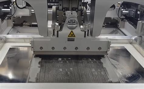
Automated Stencil Cleaning Systems for Yield Improvement
Modern PCB assembly workflows demand meticulous attention to stencil cleanliness to prevent defects like solder bridging or insufficient paste volume. Automated stencil cleaning systems have emerged as critical tools for maintaining consistent PCBA quality, particularly in high-volume production environments. These systems employ precision spray-and-vacuum mechanisms to remove residual solder paste, minimizing the risk of aperture blockages that compromise print accuracy. By integrating real-time monitoring sensors, advanced cleaners adapt cleaning cycles based on stencil contamination levels, optimizing throughput while reducing solvent waste.
Transitioning from manual cleaning to automated solutions eliminates human variability, ensuring repeatable results across thousands of SMT placements. For instance, inline cleaning modules paired with 3D SPI (Solder Paste Inspection) tools enable closed-loop process adjustments, directly linking stencil condition to downstream solder joint reliability. This synergy reduces rework rates by up to 40% in complex mixed-technology PCBA designs. Manufacturers prioritizing zero-defect manufacturing now leverage AI-powered systems that predict cleaning intervals using historical process data, further aligning with data-driven optimization frameworks outlined in earlier sections.
As stencil apertures shrink for ultra-fine-pitch components, even micron-level debris can derail solder paste deposition. Automated systems address this by combining laser ablation for hardened residues with non-abrasive wipes for delicate nano-coated stencils, extending tool lifespan. By embedding these technologies into smart factory ecosystems, producers achieve measurable yield improvements while maintaining compliance with IPC-7525 stencil design standards.
Data-Driven Process Optimization in PCB Production
Modern PCB assembly systems leverage real-time analytics to achieve unprecedented precision in PCBA manufacturing. By implementing statistical process control (SPC) tools, engineers monitor critical parameters such as solder paste viscosity, stencil alignment accuracy, and reflow oven temperature gradients. These metrics, collected through IoT-enabled sensors and vision inspection systems, feed into machine learning algorithms that predict process deviations before they impact yield.
For instance, solder paste deposition consistency improves by 18–22% when stencil printing data integrates with adaptive feedback loops. Advanced PCBA lines employ digital twins to simulate thermal profiles, reducing rework rates by correlating peak reflow temperatures with void formation patterns. Automated defect classification systems further refine process windows by analyzing thousands of solder joints per hour, identifying trends invisible to manual inspection.
Transitioning to data-centric workflows requires harmonizing PCB assembly equipment with unified analytics platforms. This approach not only elevates first-pass yield but also extends stencil lifecycles by optimizing cleaning cycles based on paste residue accumulation rates. As production scales, these strategies ensure process capability indices (Cpk) remain above 1.67, meeting stringent reliability benchmarks for high-performance electronics.
Conclusion
Implementing advanced stencil PCB assembly strategies requires a holistic approach that integrates precision engineering with data-driven decision-making. As modern PCBA processes demand tighter tolerances and higher reliability, manufacturers must prioritize solder paste optimization and thermal profiling to eliminate defects like bridging or cold joints. The adoption of automated stencil cleaning systems not only extends tool longevity but also ensures consistent paste deposition across high-volume production runs.
Critical to success is the alignment of precision stencil design with material selection guidelines, which directly impacts solder joint integrity and assembly yield. By leveraging advanced inspection methods, such as 3D AOI or X-ray analysis, teams can detect micron-level inconsistencies before they escalate into field failures. Furthermore, process control strategies rooted in real-time monitoring enable rapid adjustments to environmental variables or machine parameters, maintaining process stability even in complex PCB assembly environments.
Ultimately, achieving reliable PCBA outcomes hinges on balancing technological investments with operator expertise. From data-driven optimization to defect prevention protocols, each element contributes to a manufacturing ecosystem capable of delivering high-performance electronics with repeatable quality.
FAQs
How does stencil design impact PCB assembly quality?
Precision in aperture geometry and stencil thickness ensures optimal solder paste deposition, minimizing defects like bridging or insufficient solder. Advanced PCBA workflows use laser-cut stencils with ±10µm tolerance for high-density components.
What process controls prevent defects in PCB assembly?
Real-time solder paste inspection (SPI) and automated optical inspection (AOI) systems detect deviations early. Pairing these with statistical process control (SPC) reduces rework rates by up to 40% in PCBA lines.
Why is thermal profiling critical for reflow soldering?
A ramp-to-peak profile with controlled soak zones prevents tombstoning and cold joints. For lead-free PCB assembly, maintaining a peak temperature of 240–250°C ensures proper intermetallic bonding without damaging components.
How do automated cleaning systems enhance stencil longevity?
Closed-loop ultrasonic cleaning with VOC-free solvents removes >99.8% of solder paste residue. This extends stencil service life by 3–5x compared to manual wiping, directly improving PCBA yield rates.
Optimize Your Production Line Today
For tailored PCB assembly solutions integrating these advanced strategies, please click here to consult our PCBA engineering team.


