Altium assembly layer
Understanding The Altium Assembly Layer: A Comprehensive Guide
In the realm of electronic design automation, Altium Designer stands out as a powerful tool that facilitates the creation of complex printed circuit boards (PCBs). Among its many features, the assembly layer plays a crucial role in ensuring that the transition from design to physical assembly is seamless and efficient. Understanding the Altium assembly layer is essential for designers who aim to produce high-quality, manufacturable PCBs.
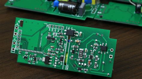
The assembly layer in Altium Designer serves as a blueprint for the assembly process, providing detailed information about the placement and orientation of components on a PCB.
This layer is distinct from other layers, such as the copper or silkscreen layers, as it is specifically tailored to guide the assembly process rather than the electrical or aesthetic aspects of the board. By including precise component outlines, reference designators, and orientation markers, the assembly layer ensures that each component is correctly placed and oriented during the manufacturing process.
One of the primary benefits of the assembly layer is its ability to reduce errors during assembly.
By providing clear and unambiguous information, it minimizes the risk of misplacing components, which can lead to costly rework or even complete board failure. Furthermore, the assembly layer aids in the inspection process, allowing for quick verification that components are correctly positioned before soldering. This layer also facilitates communication between the design and manufacturing teams, ensuring that any potential issues are identified and addressed early in the production cycle.
In addition to its role in error reduction, the assembly layer is instrumental in optimizing the assembly process.
By clearly indicating the orientation of polarized components, such as diodes and capacitors, it helps streamline the assembly workflow, reducing the time and effort required to assemble the board. This efficiency is particularly important in high-volume production environments, where even small improvements in assembly time can lead to significant cost savings.
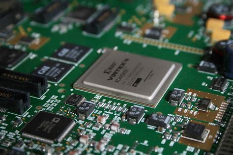
Moreover, the assembly layer is not limited to traditional surface-mount technology (SMT) components.
It also accommodates through-hole components, connectors, and other mechanical parts, providing a comprehensive view of the entire assembly. This versatility makes it an indispensable tool for designers working on a wide range of projects, from simple single-layer boards to complex multi-layer designs.
To effectively utilize the assembly layer in Altium Designer, it is important for designers to adhere to best practices.
This includes ensuring that all components have accurate and complete assembly layer data, which can often be sourced from component libraries or created manually if necessary. Additionally, designers should regularly review and update the assembly layer to reflect any changes in the design, ensuring that the information remains current and accurate throughout the design process.
In conclusion, the Altium assembly layer is a vital component of the PCB design process, providing essential information that facilitates accurate and efficient assembly. By reducing errors, optimizing workflow, and enhancing communication between design and manufacturing teams, the assembly layer plays a key role in ensuring the successful production of high-quality PCBs. As such, a thorough understanding of this layer is indispensable for designers seeking to excel in the field of electronic design automation.

Best Practices For Designing With The Altium Assembly Layer
In the realm of printed circuit board (PCB) design, the Altium assembly layer plays a crucial role in ensuring that the transition from design to physical assembly is seamless and efficient. Understanding the best practices for designing with the Altium assembly layer is essential for engineers and designers who aim to produce high-quality, reliable electronic products. This layer, often overlooked, serves as a bridge between the design and manufacturing processes, providing critical information that guides the assembly of components onto the PCB.
To begin with, it is important to recognize that the assembly layer in Altium Designer is used to convey detailed information about component placement and orientation.
This layer includes outlines of components, reference designators, and other annotations that are vital for the assembly process. Therefore, one of the best practices is to ensure that all components are accurately represented on the assembly layer. This involves verifying that each component’s outline matches its physical footprint and that reference designators are clearly visible and correctly positioned. By doing so, designers can prevent potential errors during assembly, such as incorrect component placement or orientation.
Moreover, clarity and readability are paramount when working with the assembly layer.
It is advisable to use consistent and standardized symbols and notations across the entire design. This consistency aids in reducing confusion and misinterpretation by assembly technicians. Additionally, designers should avoid overcrowding the assembly layer with excessive information. Instead, they should focus on including only the most pertinent details that are necessary for assembly. This approach not only enhances readability but also streamlines the assembly process, ultimately leading to a more efficient production cycle.
Another critical aspect of designing with the Altium assembly layer is the consideration of component polarity and orientation.
Components such as diodes, capacitors, and integrated circuits often have specific orientation requirements that must be adhered to during assembly. To address this, designers should ensure that polarity indicators and orientation markers are clearly defined on the assembly layer. This practice helps prevent assembly errors that could lead to malfunctioning circuits or even damage to the components themselves.
Furthermore, collaboration between design and manufacturing teams is essential for optimizing the use of the assembly layer.
Designers should engage in regular communication with assembly technicians to understand their needs and challenges. This collaboration can lead to valuable insights that inform design decisions, such as the placement of fiducials or the inclusion of additional assembly notes. By fostering a collaborative environment, designers can create assembly layers that are not only technically accurate but also practically useful for those involved in the manufacturing process.
In addition to these practices, leveraging the advanced features of Altium Designer can further enhance the effectiveness of the assembly layer.
For instance, utilizing automated design rule checks can help identify potential issues related to component placement and orientation before they reach the assembly stage. Additionally, taking advantage of Altium’s 3D visualization capabilities allows designers to verify the spatial arrangement of components, ensuring that there are no conflicts or interferences that could complicate assembly.
In conclusion, the Altium assembly layer is a vital component of PCB design that requires careful attention and thoughtful planning. By adhering to best practices such as ensuring accurate component representation, maintaining clarity and consistency, considering component orientation, fostering collaboration, and utilizing advanced design tools, designers can significantly improve the quality and reliability of their electronic products. These efforts not only facilitate a smoother transition from design to assembly but also contribute to the overall success of the manufacturing process.
Troubleshooting Common Issues In The Altium Assembly Layer
In the realm of electronic design automation, Altium Designer stands out as a powerful tool for creating printed circuit boards (PCBs). Among its many features, the assembly layer plays a crucial role in ensuring that the physical assembly of the PCB aligns with the design specifications. However, like any complex software, users may encounter issues when working with the assembly layer. Understanding and troubleshooting these common issues is essential for maintaining the integrity of the design and ensuring a smooth transition from digital design to physical product.
One frequent issue that designers face is the misalignment of components on the assembly layer.
This can occur due to discrepancies between the component footprints in the library and the actual components used in the design. To address this, it is imperative to verify that the component footprints in the library are accurate and up-to-date. Regularly updating the component library and cross-referencing it with manufacturer specifications can prevent such misalignments. Additionally, utilizing Altium’s footprint wizard can aid in creating precise and reliable footprints, thereby minimizing the risk of errors.
Another common problem is the omission of certain components from the assembly layer.
This often happens when components are not properly assigned to the assembly layer during the design process. To troubleshoot this, designers should ensure that all components are correctly assigned to the appropriate layers. This can be achieved by reviewing the layer stack manager and confirming that each component is visible on the assembly layer. Furthermore, employing design rule checks (DRCs) can help identify any components that may have been inadvertently excluded from the assembly layer, allowing for timely corrections.
Moreover, issues with silkscreen overlap can also arise, leading to confusion during the assembly process.
Silkscreen overlap occurs when the silkscreen markings, such as reference designators or outlines, interfere with solder pads or other critical areas on the PCB. To mitigate this, designers should carefully review the placement of silkscreen elements and adjust them as necessary to avoid overlaps. Altium Designer provides tools for adjusting silkscreen placement, which can be utilized to ensure that all markings are clear and do not interfere with the assembly process.
In addition to these issues, incorrect layer stack configurations can lead to assembly layer problems.
A well-defined layer stack is essential for ensuring that all layers, including the assembly layer, are correctly aligned and function as intended. Designers should meticulously configure the layer stack, taking into account the specific requirements of the PCB design. This includes verifying that the assembly layer is correctly positioned within the stack and that all necessary information is included.
Furthermore, communication between design and manufacturing teams is crucial in preventing assembly layer issues.
Miscommunication can lead to discrepancies between the design intent and the manufactured product. To avoid this, designers should provide clear and comprehensive documentation, including detailed assembly drawings and notes. This documentation should be reviewed and approved by both design and manufacturing teams to ensure that all parties have a mutual understanding of the design requirements.
In conclusion, while working with the Altium assembly layer can present challenges, understanding and addressing common issues can significantly enhance the design process. By ensuring accurate component footprints, proper layer assignments, clear silkscreen placement, and effective communication, designers can mitigate potential problems and facilitate a seamless transition from design to assembly. As technology continues to evolve, staying informed about best practices and leveraging Altium Designer’s robust features will be key to overcoming these challenges and achieving successful PCB designs.
Enhancing PCB Design Efficiency Using The Altium Assembly Layer
In the realm of printed circuit board (PCB) design, efficiency and precision are paramount. As technology continues to advance, the demand for more complex and compact electronic devices grows, necessitating innovative solutions in PCB design. One such solution is the utilization of the Altium Assembly Layer, a feature within the Altium Designer software that significantly enhances the design process. By understanding the role and benefits of the Altium Assembly Layer, designers can streamline their workflows and improve the overall quality of their PCB projects.
The Altium Assembly Layer serves as a critical component in the PCB design process, providing a dedicated space for assembly-related information.
This layer is distinct from other layers, such as the signal or power layers, as it focuses specifically on the assembly and manufacturing aspects of the PCB. By incorporating this layer into the design, engineers can ensure that all necessary assembly details are clearly communicated to the manufacturing team, thereby reducing the likelihood of errors and rework.
One of the primary advantages of using the Altium Assembly Layer is its ability to convey detailed component placement information.
This includes the exact position and orientation of each component on the PCB, which is crucial for accurate assembly. By providing a visual representation of component placement, the assembly layer helps to eliminate ambiguity and ensures that components are correctly positioned during the manufacturing process. This level of precision is particularly important for high-density PCBs, where even minor misalignments can lead to significant performance issues.
In addition to component placement, the Altium Assembly Layer also facilitates the inclusion of assembly notes and instructions.
These notes can cover a wide range of topics, from specific soldering requirements to the use of particular tools or techniques. By embedding this information directly into the PCB design, engineers can ensure that all relevant assembly instructions are readily accessible to the manufacturing team. This not only enhances communication but also helps to prevent misunderstandings that could lead to costly delays or defects.
Moreover, the Altium Assembly Layer supports the integration of additional design elements, such as fiducials and tooling holes, which are essential for automated assembly processes.
Fiducials serve as reference points for pick-and-place machines, enabling precise component placement, while tooling holes assist in the alignment and handling of the PCB during assembly. By incorporating these elements into the assembly layer, designers can optimize their PCBs for automated manufacturing, thereby increasing production efficiency and reducing labor costs.
Furthermore, the Altium Assembly Layer plays a vital role in design verification and validation.
By providing a comprehensive overview of the assembly process, this layer allows engineers to conduct thorough reviews and identify potential issues before the PCB is sent to production. This proactive approach to design verification helps to minimize the risk of errors and ensures that the final product meets all specified requirements.
In conclusion, the Altium Assembly Layer is an invaluable tool for enhancing PCB design efficiency. By offering a dedicated space for assembly-related information, this layer facilitates clear communication between design and manufacturing teams, supports automated assembly processes, and aids in design verification. As a result, engineers can produce high-quality PCBs with greater accuracy and speed, ultimately meeting the demands of today’s fast-paced technological landscape. Embracing the capabilities of the Altium Assembly Layer is a strategic move for any designer seeking to optimize their PCB design process and achieve superior results.


