Balanced PCB Stackup Design Methodology
Introduction
Printed Circuit Board (PCB) stackup design is a critical factor in determining the performance, reliability, and manufacturability of modern electronic systems. As signal speeds continue to increase and form factors shrink, implementing a balanced stackup has become essential for achieving optimal electrical performance while maintaining mechanical stability. This paper explores the methodology for creating balanced PCB layer stackups, covering fundamental concepts, design considerations, material selection, and practical implementation techniques.
Fundamentals of PCB Stackup
Definition and Importance
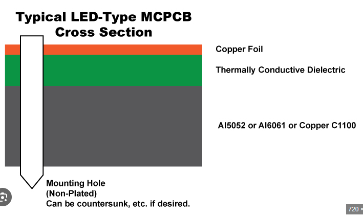
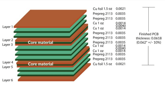
A PCB stackup refers to the arrangement of copper layers and insulating materials that make up a circuit board. A balanced stackup is one where the layer arrangement, material distribution, and copper weighting are symmetrical about the central plane of the board. This symmetry provides several key benefits:
- Mechanical Stability: Reduces warpage and twisting during manufacturing and operation
- Improved Signal Integrity: Maintains consistent impedance characteristics
- Thermal Management: Even heat distribution across the board
- Manufacturing Reliability: Minimizes production defects and improves yield
Basic Stackup Configurations
Common balanced stackup configurations include:
- 4-Layer Board: Typically arranged as Signal – Ground – Power – Signal
- 6-Layer Board: Common arrangements include:
- S – G – S – P – G – S
- S – G – S – S – G – S (for high-speed designs)
- 8-Layer Board: Often configured as:
- S – G – S – P – G – S – G – S
- S – G – S – S – G – P – G – S
Key Considerations for Balanced Stackup Design
Layer Symmetry
The foundation of balanced stackup design lies in creating symmetry about the board’s center. This involves:
- Layer Pairing: Matching signal layers with similar characteristics on opposite sides
- Material Balance: Using identical prepreg and core materials in symmetrical positions
- Copper Weight Distribution: Maintaining equivalent copper thicknesses in corresponding layers
Impedance Control
Maintaining consistent characteristic impedance is crucial for signal integrity:
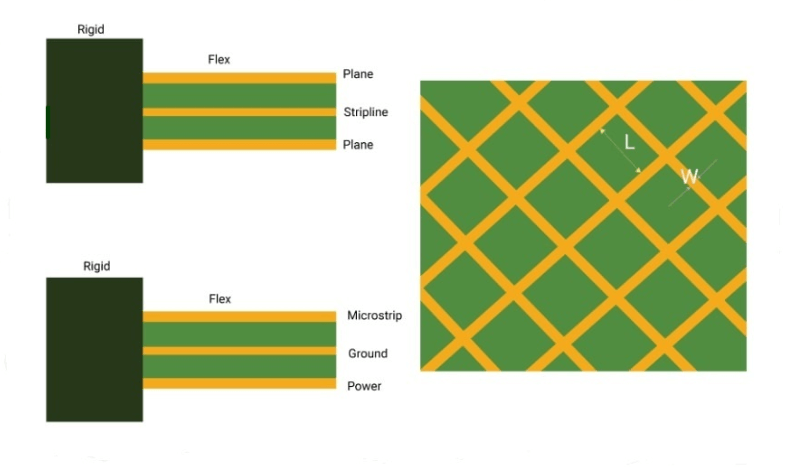
- Microstrip vs. Stripline: Surface traces (microstrip) versus embedded traces (stripline) have different impedance characteristics
- Dielectric Thickness: The distance between signal and reference planes affects impedance
- Trace Geometry: Width and thickness must be adjusted based on layer position
Power Delivery Network (PDN) Design
A robust PDN is essential for proper circuit operation:
- Power-Ground Pairing: Tight coupling between power and ground planes reduces impedance
- Decoupling Strategy: Proper placement of decoupling capacitors based on stackup
- Split Planes: Careful design when multiple voltages share the same layer
Signal Layer Allocation
Optimal signal layer arrangement improves performance:
- High-Speed Signals: Prefer stripline layers for critical signals
- Clock Routing: Dedicated layers or careful spacing from other signals
- Cross-Talk Mitigation: Orthogonal routing on adjacent layers
Material Selection for Balanced Stackups
Dielectric Materials
Key properties to consider:
- Dielectric Constant (Dk): Affects signal propagation speed and impedance
- Dissipation Factor (Df): Impacts signal loss at high frequencies
- Thermal Stability: Important for reliability under temperature variations
Copper Foil Characteristics
- Electrodeposited vs. Rolled Annealed: Different surface roughness affects high-frequency performance
- Weight Selection: Typical options include 0.5 oz, 1 oz, and 2 oz copper
- Surface Treatment: Considerations for final finish (ENIG, HASL, immersion silver, etc.)
Advanced Materials
For high-frequency applications:
- Low-Loss Materials: Such as Rogers, Isola, or Panasonic materials
- Hybrid Stackups: Combining standard FR-4 with specialty materials
- Thermal Management Materials: For power electronics applications
Design Methodology
Step 1: Define Requirements
- Board Functionality: Digital, analog, RF, or mixed-signal
- Performance Needs: Speed, bandwidth, and signal integrity requirements
- Mechanical Constraints: Board thickness, flexibility needs
- Manufacturing Capabilities: Available materials and processes
Step 2: Determine Layer Count
Based on:
- Component Density: Number and pitch of components
- Routing Complexity: Signal count and escape routing needs
- Power Requirements: Number of voltage domains
Step 3: Create Symmetrical Stackup
- Center About Midplane: Arrange layers symmetrically around the center
- Balance Copper Weights: Match corresponding layers
- Mirror Material Build: Use identical materials in mirrored positions
Step 4: Assign Layer Functions
- Signal Layers: Distribute based on speed and sensitivity
- Plane Layers: Optimize for power delivery and return paths
- Mixed Layers: Carefully plan when signals share space with planes
Step 5: Calculate Impedances
- Target Impedances: Typically 50Ω single-ended, 100Ω differential
- Adjust Trace Geometry: Width and spacing based on layer position
- Verify with Field Solvers: Use simulation tools for accuracy
Step 6: Finalize Materials
- Select Core/Prepreg: Based on dielectric needs
- Determine Copper Weights: Balance electrical and thermal needs
- Consider Special Materials: For critical signals or sections
Practical Implementation Guidelines
Manufacturing Considerations
- Fabrication Tolerances: Account for ±10% material thickness variations
- Registration Accuracy: Layer-to-layer alignment capabilities
- Copper Balance: Ensure etch patterns don’t create imbalance
Testing and Verification
- Impedance Testing: Coupon designs for verification
- Cross-Section Analysis: For critical boards
- Signal Integrity Measurements: TDR and eye diagram tests
Common Pitfalls to Avoid
- Asymmetric Material Distribution: Leading to warpage
- Inadequate Plane Pairing: Causing PDN issues
- Improper Layer Sequencing: Resulting in crosstalk problems
- Ignoring Manufacturing Realities: Designing beyond fabrication capabilities
Advanced Techniques
High-Speed Design Considerations
- Differential Pair Routing: Careful spacing and length matching
- Via Optimization: Minimizing stub lengths
- Return Path Management: Ensuring continuous reference planes
EMI Reduction Strategies
- Shielding Layers: Strategic placement of ground layers
- Edge Treatment: Mitigating edge radiation
- Split Plane Design: Careful implementation for mixed-signal boards
HDI Stackups
- Microvia Technology: Enabling higher density
- Sequential Lamination: For complex HDI designs
- Any-Layer Interconnect: Most flexible HDI approach
Case Studies
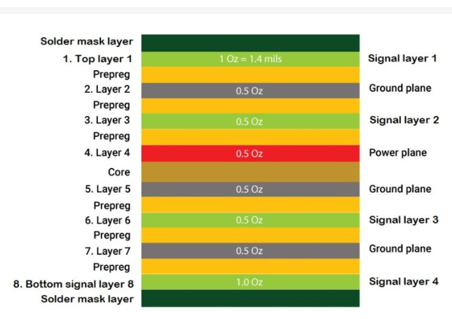
Case 1: 8-Layer General Purpose Board
Analysis of a common balanced stackup:
- Layer 1: Signal (Top)
- Layer 2: Ground
- Layer 3: Signal
- Layer 4: Power
- Layer 5: Ground
- Layer 6: Signal
- Layer 7: Power
- Layer 8: Signal (Bottom)
Case 2: 12-Layer High-Speed Board
Examination of a high-performance design:
- Special considerations for signal layers
- Multiple ground plane strategy
- Low-loss material incorporation
Case 3: Mixed-Signal Design
Balancing analog and digital requirements:
- Partitioning strategies
- Ground plane management
- Noise isolation techniques
Future Trends
Emerging Materials
- Ultra-Low Loss Dielectrics: For millimeter-wave applications
- Embedded Passives: Integrating components within the stackup
- Flex-Rigid Combinations: For advanced packaging
3D Integration
- Package-on-Package: Stackup considerations
- Silicon Interposers: Mixed technology boards
- Advanced Thermal Management: For 3D-IC integration
AI-Assisted Design
- Automated Stackup Optimization: Machine learning algorithms
- Manufacturing Yield Prediction: AI-based analysis
- Performance Simulation: Rapid what-if analysis
Conclusion
Balanced PCB stackup design is a multidimensional engineering challenge that requires careful consideration of electrical, mechanical, and manufacturing requirements. By following a systematic methodology that emphasizes symmetry, proper material selection, and attention to signal integrity principles, designers can create robust stackups that meet the demanding requirements of modern electronic systems. As technology continues to advance, the importance of proper stackup design will only increase, requiring designers to stay abreast of new materials, techniques, and tools in this critical aspect of PCB development.
The balanced stackup approach outlined in this paper provides a framework for creating reliable, high-performance PCB designs that can be manufactured consistently while meeting all operational requirements. By understanding and applying these principles, engineers can avoid common pitfalls and create optimized designs for their specific applications.