CADENCE PCB Design Technology Solutions
Layout Planning and Layout
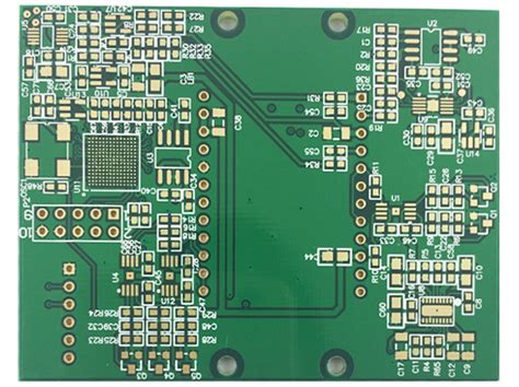
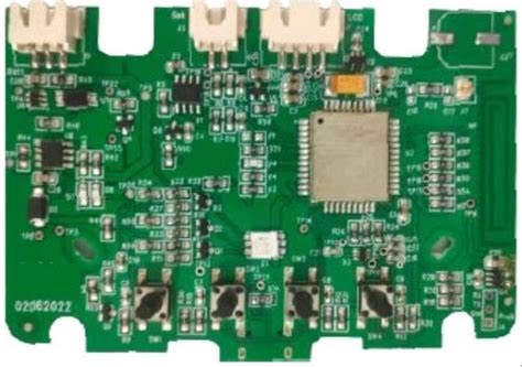
Constraint and rule-driven methods facilitate powerful and flexible layout functions, including interactive and automatic component layout. Engineers or designers can assign components or subcircuits to specific areas during the design input or layout planning stage. Components can be filtered or selected by REF, package type, related signal name, part number or schematic diagram/page number. There are thousands of components on today’s circuit boards, which require precise management.
Through real-time device assembly analysis and feedback
it is possible to consider and meet EMS rules when assembling devices as a whole to improve the designer’s design speed and efficiency. DFA (Design for Assembly) Analysis. Allegro PCB Design XL and GXL provide real-time DFA rule checking during interactive component placement. Based on a two-dimensional spreadsheet of device type and package arrangement, DFA can check in real time whether the device’s edge-to-edge, edge-to-end or end-to-end distance violates the minimum requirements, allowing PCB designers to place components synchronously to achieve optimal routability, producibility and signal timing requirements.
Strategic Planning and Design Intent (GRE, global routing environment)
Highly constrained, high-density designs dominated by bus interconnects can spend a lot of time on strategic planning and routing. Coupled with today’s component density issues, new signal standards and specific topology requirements, traditional CAD tools and technologies are no longer sufficient to capture the designer’s specific routing intent requirements.
Global routing environment technology, limited to Allegro PCB Design GXL, provides the technology and methods needed to capture and implement designer intent.
Through an interactive process planning architecture and global routing engine, users can apply their experience and design intent to the tools that understand what they need in the first place. This solution accomplishes this goal. Allow users to create extracted interconnect data, through the interconnect process planning framework, and quickly converge into a solution, and process it with the global routing engine.
The interconnect extraction function reduces the number of components that the system needs to process
reducing the number of components from the possible thousands to hundreds, thereby greatly reducing the need for manual operations. In addition, it also reduces the number of visible devices in the interconnect process planning framework, and reduces the number of components they need to manage physically.
Using the data extraction function, the routing process can be completed quickly by comparing the extracted data to see whether the routing space is consistent with the user’s design intent. Therefore, the routing engine can solve the routing details and implement specific intentions. Users do not need to stare at the screen all the time to solve the routing problem. This represents a significant simplification of current design tools, allowing users to complete their designs faster and more effectively. Now users can converge into a successful interconnect solution faster and easier than ever before, shortening the design cycle time through improved efficiency and design speed.
Design Split
Design teams are increasingly dispersed around the world, which makes the related issues of shortening design cycle time more complicated. Manual operations to solve multi-user problems are very time-consuming, slow and prone to errors. PCB design split technology, provided by Allegro PCB design layer, provides a multi-user, synchronous design method, achieving faster time to market and reducing layout time.
Using this technology, multiple designers working on a layout diagram can call a single database together, no matter how far apart the groups are. Design split technology allows designers to split the design into multiple parts or areas, which can be planned and edited by multiple design team members. In this way, all designers can view all the divided parts, update the design window, and monitor the status and progress of other users’ parts, which can greatly shorten the entire design cycle and accelerate the design process.
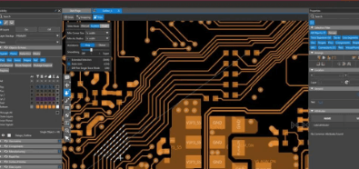
Interactive Routing Editing
The interactive routing feature of the PCB editor provides powerful, interactive functions that enable controlled automation to maintain user operation while maximizing routing efficiency. Real-time, graphical, any-angle push routing allows users to choose push priority, wrap priority, or wrap only mode.
Push priority mode allows users to build the most appropriate interconnect path, and the real-time, graphical router automatically solves dynamic push obstacles. Routing automatically jumps obstacles such as pins or vias.
When you need to build a data bus, the wire priority mode is the perfect solution. In wrap priority mode, the router diagram The shape will follow other interconnects as priority, and will only push or jump over obstacles when there is no choice. The surround-only type is executed like the surround priority mode, but there is no intention to push other etching targets.
The real-time embedded graphic routing engine can optimize routing by pushing obstacles, or following copper obstacles, while dynamically jumping vias or component pins. When editing, designers can use a real-time graphical window that can display timing gaps under interconnects with high-speed constraints. Interconnect routing also provides the ability to perform group routing on multiple lines, as well as the ability to interactively adjust lines with high-speed length or delay constraints, as shown in Figure 3.