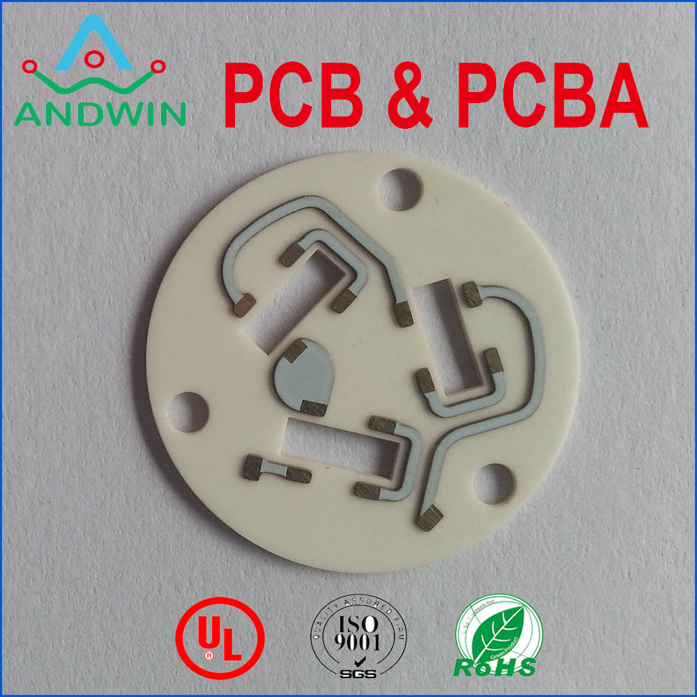
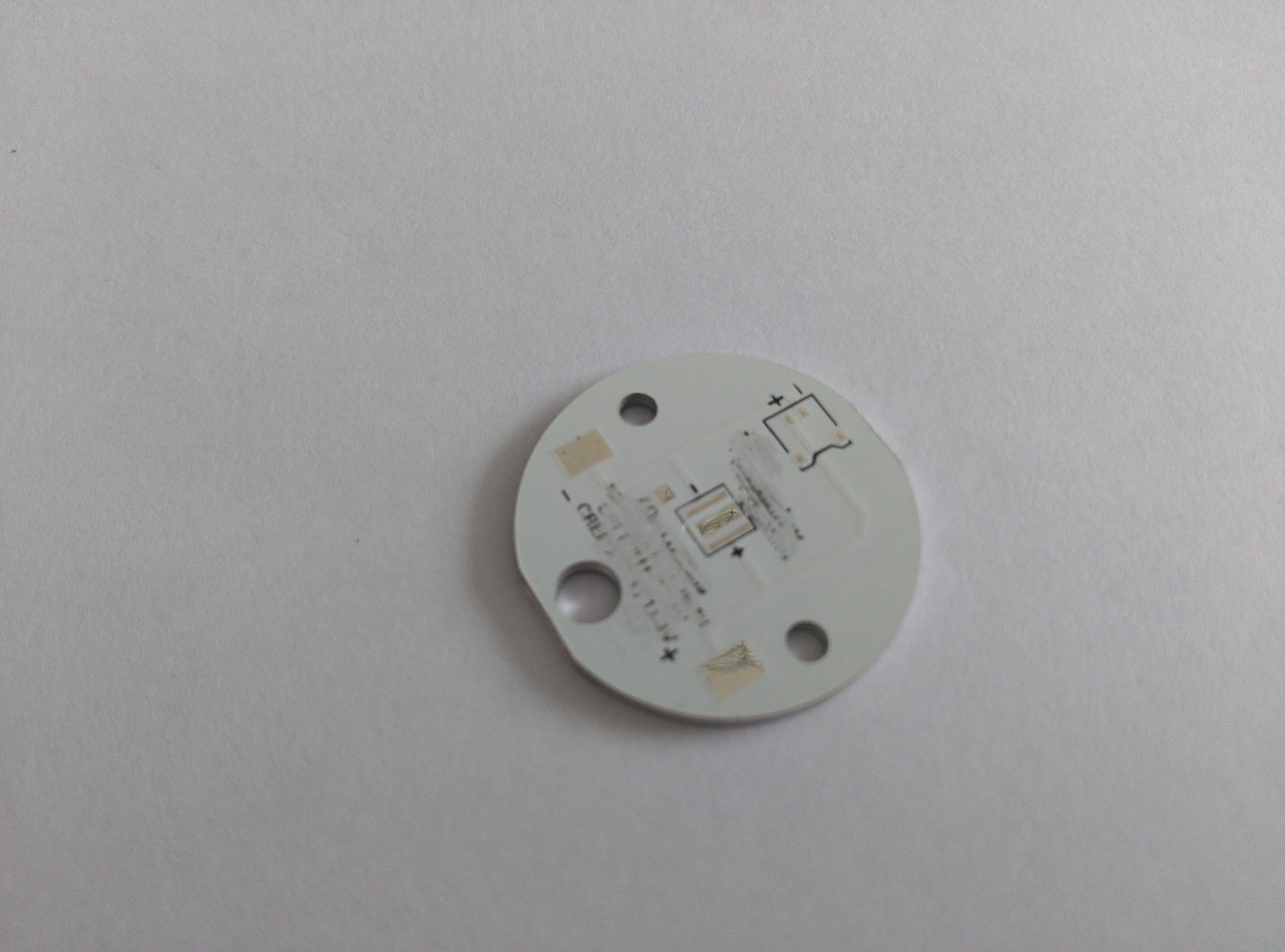
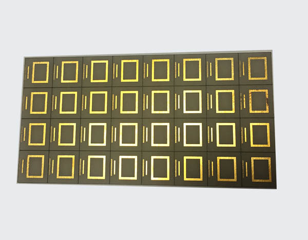
Ceramic PCB list – quality Ceramic PCB privided ceramic pcb process
In this letter, we will be discussing the process of ceramic PCB manufacturing. Ceramic
PCBs are a type of printed circuit board that are made using ceramic materials instead
of traditional materials like fiberglass or plastic. Ceramic PCBs are becoming increasingly
popular due to their superior thermal properties, high electrical insulation, and high mechanical strength.
The process of ceramic PCB manufacturing involves several steps, including design,
material selection, printing, firing, and finishing. Let’s take a closer look at each of these steps.

Design:
The first step in ceramic PCB manufacturing is the design phase. This involves
creating a digital layout of the circuit board using specialized software. The design
must take into account the electrical properties of the circuit, as well as the physical
dimensions of the board.
Material Selection:
Once the design is complete, the next step is to select the appropriate ceramic material
for the PCB. The most commonly used ceramic materials for PCBs are aluminum oxide
(Al2O3), aluminum nitride (AlN), and silicon carbide (SiC). Each material has its
own unique properties and is suitable for different applications.

Printing:
After the material has been selected, the next step is to print the circuit onto the
ceramic substrate. This is done using a specialized printer that can apply the
conductive ink to the ceramic substrate with high precision. The ink used for printing is
typically a silver or copper-based material that provides good electrical conductivity.
Firing:
Once the circuit has been printed onto the ceramic substrate, the next step is to fire
the board. This involves subjecting the board to high temperatures in a kiln or furnace.
The firing process helps to bond the conductive ink to the ceramic substrate,creating a
strong and durable circuit.
Finishing:
The final step in ceramic PCB manufacturing is finishing. This involves adding any necessary
components to the board, such as resistors, capacitors, and diodes. The components are soldered
onto the board using a specialized soldering process that ensures a strong and reliable connection.

In conclusion, the process of ceramic PCB manufacturing involves several steps,
including design, material selection, printing,firing, and finishing. Each step is critical
to the overall quality and performance of the finished circuit board. Ceramic PCBs offer
several advantages over traditional PCBs, including superior thermal properties, high
electrical insulation, and high mechanical strength. As a result, they are becoming
increasingly popular in a wide range of applications, from aerospace and defense to
medical devices and consumer electronics.
Thank you for taking the time to read this letter. If you have any questions or would
like to learn more about ceramic PCB manufacturing, please do not hesitate to contact us.


