Comprehensive Testing Methods for Bare PCB Boards
Introduction
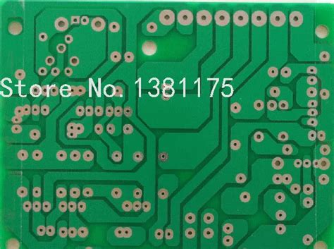
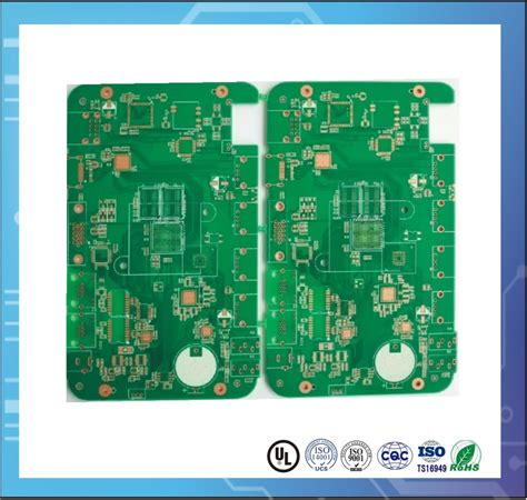
Printed Circuit Boards (PCBs) are the backbone of modern electronic devices, providing mechanical support and electrical connections between components. Before assembling components onto a PCB, it is crucial to test the bare board to ensure its functionality, reliability, and compliance with design specifications. Bare PCB testing involves verifying continuity, insulation resistance, impedance, and structural integrity. This article explores various testing methods for bare PCBs, including visual inspection, automated optical inspection (AOI), electrical testing, and advanced techniques like flying probe and boundary scan testing.
1. Visual Inspection
Visual inspection is the most basic yet essential method for identifying obvious defects in a bare PCB.
Key Checks:
- Alignment and registration – Ensuring layers are properly aligned.
- Surface defects – Scratches, dents, or uneven copper traces.
- Solder mask issues – Incomplete coverage or misalignment.
- Drilling accuracy – Hole placement and size correctness.
While manual inspection is cost-effective, it is time-consuming and prone to human error. Automated Optical Inspection (AOI) systems are increasingly used for higher accuracy.
2. Automated Optical Inspection (AOI)
AOI systems use high-resolution cameras and image processing software to detect defects in bare PCBs.
Advantages:
- High-speed inspection – Faster than manual checks.
- Precision – Detects minute defects (e.g., micro-cracks, shorts).
- Repeatability – Consistent performance without fatigue.
Limitations:
- Limited to surface defects – Cannot detect internal layer issues.
- Requires proper lighting and calibration – False positives/negatives possible.
3. Electrical Testing
Electrical testing ensures that the PCB meets connectivity and insulation requirements.
3.1 Continuity Testing (Short Testing)
- Checks for unintended connections (shorts) between traces.
- Uses a low-voltage current to verify open and short circuits.
3.2 Insulation Resistance Testing
- Measures resistance between isolated conductors to ensure no leakage.
- High-voltage testing (typically 100-500V) is applied.
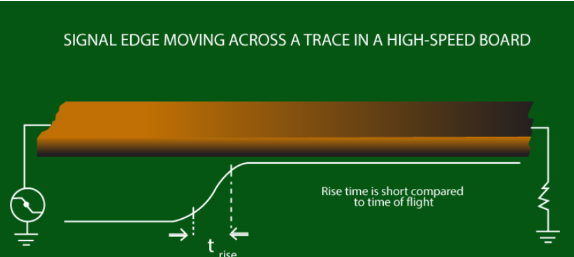
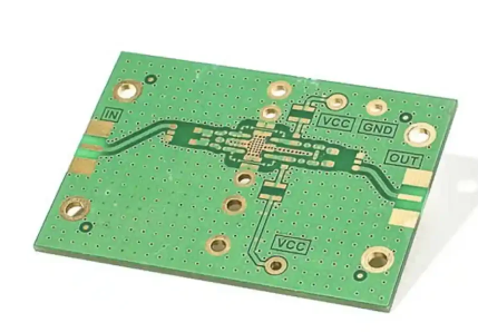
3.3 Impedance Testing
- Critical for high-frequency PCBs (e.g., RF, high-speed digital circuits).
- Time-domain reflectometry (TDR) is commonly used for impedance measurement.
4. Flying Probe Testing
Flying probe testers are versatile and do not require custom fixtures, making them ideal for prototype and low-volume production.
How It Works:
- Movable probes test different points on the PCB sequentially.
- Measures resistance, capacitance, and inductance.
Advantages:
- No need for test fixtures – Reduces setup costs.
- Flexible for different PCB designs – Suitable for prototypes.
Disadvantages:
- Slower than bed-of-nails testing – Not ideal for mass production.
5. Bed-of-Nails Testing (Fixture-Based Testing)
A bed-of-nails tester uses a custom fixture with spring-loaded pins to contact test points on the PCB simultaneously.
Advantages:
- High-speed testing – Suitable for mass production.
- Comprehensive coverage – Tests multiple points at once.
Disadvantages:
- High initial cost – Requires custom fixtures for each PCB design.
- Maintenance needed – Pins can wear out over time.
6. Boundary Scan Testing (JTAG)
Boundary scan testing, based on IEEE 1149.1 (JTAG), is used for complex PCBs with high-density components.
How It Works:
- Uses dedicated test access ports (TAPs) to check interconnections.
- Particularly useful for testing BGAs and other hard-to-reach components.
Advantages:
- No physical probes needed – Reduces mechanical wear.
- Tests hidden connections – Effective for multilayer PCBs.
Limitations:
- Requires JTAG-compliant components – Not all PCBs support it.
7. X-Ray Inspection
X-ray inspection is used to detect internal defects in multilayer PCBs, such as:
- Voiding in vias – Incomplete plating or air pockets.
- Misaligned layers – Detected through cross-sectional imaging.
Applications:
- High-reliability PCBs (aerospace, medical devices).
- Fine-pitch components (BGAs, microvias).
8. Environmental Stress Testing
Some PCBs undergo environmental testing to ensure reliability under harsh conditions:
- Thermal cycling – Checks expansion/contraction effects.
- Humidity testing – Detects moisture absorption issues.
Conclusion
Testing bare PCBs is a critical step in ensuring product quality and reliability. Depending on the application, different testing methods—such as AOI, flying probe, bed-of-nails, and boundary scan—can be employed. Combining multiple techniques provides comprehensive validation, reducing the risk of defects in the final product. As PCB technology advances, testing methods continue to evolve, incorporating AI-driven inspection and advanced signal integrity analysis for higher precision.
By implementing rigorous testing protocols, manufacturers can minimize failures, improve yield, and deliver high-performance PCBs for various industries.