Design points of DC/DC converter in switch mode power supply
Introduction
As the core component of switch mode power supply (SMPS), the design of DC/DC converter has a vital impact on the performance, efficiency, stability and reliability of the whole power system. With the rapid development of electronic technology, DC/DC converters are increasingly used in various fields, especially in occasions with high requirements for power quality, such as communication equipment, data centers, electric vehicles, etc. This article will start from the basic principles of DC/DC converters and explore its design points in switch mode power supply, in order to provide valuable reference for relevant engineers.
Basic principles of DC/DC converters
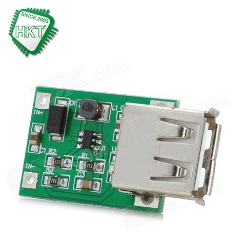
The main function of DC/DC converters is to convert one DC voltage into another DC voltage. In a switch mode power supply, the DC/DC converter converts the input DC voltage into a high-frequency pulse voltage by controlling the on and off of the switching element (such as MOSFET), and then processes it through components such as transformers, rectifiers and filters to finally output a stable DC voltage. This conversion method has the advantages of high efficiency, small size and light weight, so it has been widely used in modern electronic devices.
Design points
- Selection of topology
DC/DC converters have various topologies, such as buck, boost, buck-boost, forward, flyback, etc. When selecting a topology, it is necessary to consider various factors based on actual application requirements, such as input and output voltage range, power requirements, efficiency requirements, etc. For example, for applications that require voltage reduction, the buck topology is a more appropriate choice; while for applications that require voltage increase, the boost or buck-boost topology can be selected.
- Selection of switching elements
Switching elements are the core components of DC/DC converters, and their performance directly affects the efficiency and reliability of the converter. When selecting switching elements, it is necessary to consider parameters such as withstand voltage, current resistance, switching speed, and on-resistance. At present, MOSFET has become a commonly used switching element in DC/DC converters due to its high switching speed, low on-resistance, and good thermal stability. In addition, it is necessary to select a suitable package form according to the specific application scenario to ensure the heat dissipation performance and reliability of the switching components.
- Electromagnetic compatibility design
Electromagnetic compatibility (EMC) is an important aspect that cannot be ignored in the design of DC/DC converters. During the high-frequency switching process, the DC/DC converter will generate a large amount of electromagnetic interference (EMI), which may have adverse effects on other electronic devices. Therefore, a series of measures need to be taken during the design process to reduce EMI, such as reasonable layout of routing, use of shielding materials, and addition of filtering components. In addition, EMC testing of the DC/DC converter is required to ensure that it meets relevant standards and requirements.
- Thermal design
Thermal design is another key link in the design of DC/DC converters. Since the switching components generate a lot of heat during the high-frequency switching process, if the heat dissipation is poor, the temperature of the switching components will rise, which will affect its performance and reliability. Therefore, the heat dissipation problem needs to be fully considered during the design process, such as selecting a suitable heat sink, using heat pipe heat dissipation technology, and optimizing the PCB layout. At the same time, the DC/DC converter needs to be thermally tested to ensure that it can maintain good heat dissipation performance during long-term operation.
- Loop design
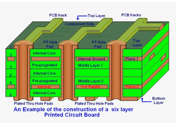
Loop design is an important part of DC/DC converter design. During high-frequency switching, signal traces and their return paths form loops, which generate electromagnetic radiation and affect the performance of the converter. In order to reduce the loop area and reduce electromagnetic radiation, a series of measures need to be taken to optimize the loop design, such as placing the signal trace close to its return path, using ground planes/closely spaced power planes to minimize the loop area, etc. In addition, attention should be paid to the parasitic inductance problem in the loop to avoid its impact on the performance of the converter.
- Feedback and control
Feedback and control are the key to achieving stable output of DC/DC converters. During the design process, it is necessary to select appropriate feedback components (such as resistors, capacitors, etc.) and feedback network structures to ensure that the converter can accurately track changes in output voltage or current and make corresponding adjustments. At the same time, it is also necessary to design a reasonable control algorithm to optimize the dynamic response and stability of the converter. At present, digital control technology has been widely used in DC/DC converters, and more precise and flexible control can be achieved through digital control algorithms.

Summary
The design of DC/DC converters in switch-mode power supplies is a complex and delicate process that requires comprehensive consideration of topology selection, switch element selection, electromagnetic compatibility design, thermal design, loop design, feedback and control, and other aspects. Through reasonable design and optimization, efficient, stable and reliable operation of DC/DC converters can be achieved, providing high-quality power supply guarantee for modern electronic devices. With the continuous development of electronic technology, the design of DC/DC converters will continue to innovate and improve to meet more diverse application needs.


